Table of Contents
Advertisement
Quick Links
Advertisement
Table of Contents

Related Manuals for Propox MMnet102

Summary of Contents for Propox MMnet102
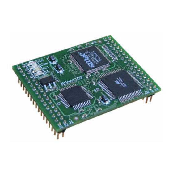
- Page 1 Ethernet Minimodule User’s Manual REV 0.9 Many ideas one solution...
-
Page 2: Table Of Contents
Contents 1 INTRODUCTION ............................3 .............................. 4 PPLICATIONS ..............................4 EATURES CONSTRUCTION OF THE MODULE ....................5 ............................5 LOCK DIAGRAM ............................6 ODULE PIN ......................13 MEGA MICROCONTROLLER LAN91C111..................... 13 THERNET CONTROLLER ..........................14 EMORY CONTROLLER ............................19 MEMORY .......................... -
Page 3: Introduction
Introduction Thank you very much for having bought our minimodule MMnet102. It was created with the idea of facilitating the communication of microprocessor systems through the Internet/Ethernet networks. The heart of the module is the RISC Atmega128 microcontroller with 128kB of program memory and 128kB of (external) RAM memory, co-operating with the Ethernet LAN91C111 controller (100BaseTX). -
Page 4: Applications
Applications The MMnet102 minimodule can be used as a design base for electronic circuits co-operating from the Ethernet/Internet network, covering the following areas of interest: • Industrial remote controlling and monitoring systems • Telemetry • Intelligent buildings • Alarm systems •... -
Page 5: Construction Of The Module
2 Construction of the module Block diagram The block diagram of the MMnet102 minimodule is shown in the drawing: memory controller PORTE 128kB RAM LAN91C111 ATmega128 PORTF EEPROM PORTB PORTD DataFlash 1 DataFlash 2 16MHz 32kHz 32kHz Batt Figure 1 Block diagram of the MMnet102 minimodule. -
Page 6: Module Pin-Out
Individual orders coding: MMnet102 – r – b – f – x – e 0 - without LAN91C111 0 – without RTC 0 - without DataFlash memory 1 - with LAN91C111 1 - RTC DS1307 1 - 32Mb DataFlash 2 - 2x32Mb DataFlash 0 –... - Page 7 Name Name Function in MMnet102 Function in MMnet102 SEL2 SEL1 Interrupt from PE7/ INT7 PE6/ INT6 LAN91C111 (optionally) Interrupt from PE5/ INT5 PE4/ INT4 LAN91C111 PE3/ AC- PE2/ AC+ PE1/ PDO/TxD PE0/ PDI/RxD PF7/ ADC7/TDI PF6/ ADC6/TDO PF5/ ADC5/TMS PF4/ ADC4/TCK...
- Page 8 Function Alt. function Description Data bus. Allows connecting externals peripherals mapped in microcontroller address space. Peripheral addressing is done with use of SEL1, SEL2 and/or A0, A1, #WR, #RD outputs. Lowest two bits of address bus. Allows addressing 4 input and 4 output registers.
- Page 9 PE1 – general purpose digital I/O Alternative functions: PDO – SPI Serial Programming Data Output. During Serial PDO/TxD Program Downloading, this pin is used as data output line for the ATmega128. TXD0 – UART0 Transmit pin. PE0 – general purpose digital I/O Alternative functions: PDI –...
- Page 10 Function Alt. function Description Power supply input +5V Ground Output of +3.3V voltage from internal regulator. Can be used to +3.3V power external peripherals, which requires +3.3V. Ground Battery voltage sustaining the operation of the RTC clock. If a battery is mounted on the module, this lead-out can be used as a Vbat source of power for peripherals external to the module.
- Page 11 PD1 – general purpose digital I/O Alternative functions: INT1 – External Interrupt source 1. The PD1 pin can serve as an external interrupt source to the MCU. SDA – Two-wire Serial Interface Data: When the TWEN bit in #INT1/SDA TWCR is set (one) to enable the Two-wire Serial Interface, pin PD1 is disconnected from the port and becomes the Serial Data I/O pin for the Two-wire Serial Interface.
- Page 12 PB2 – general purpose digital I/O Alternative functions: MOSI – SPI Master Data output, Slave Data input for SPI channel. When the SPI is enabled as a slave, this pin is MOSI configured as an input regardless of the setting of DDB2. When the SPI is enabled as a master, the data direction of this pin is controlled by DDB2.
-
Page 13: Atmega128 Microcontroller
ATmega128 microcontroller • High-performance RISC architecture, 121 instructions (most single clock cycle execution), 16 MIPS at 16MHz • 128 KBytes of Flash memory • 4K Bytes of SRAM memory • 4K Bytes of EEPROM • SPI Master/Slave interface • Four internal timers/counters 8/16bit •... -
Page 14: Memory Controller
The address space of the microcontroller under the addresses 0xFF00 to 0xFFFF contains an area reserved for MMnet102. It has two registers: a configuration and bank select registers, an area for the peripherals controlled by the SEL outputs and an area for the Ethernet controller. - Page 15 The MMnet102_BANKSR register contained under the address 0xFF00 is used for the choice of an active RAM memory bank. The contents of this register have a meaning only when mode 1 of the memory controller is chosen. The register has only four lowest bits, during readout the remaining bits (4 – 7) have the value „0” and the value written into them has no meaning.
- Page 16 In this mode the external RAM memory and the Ethernet controller are not accessible. SEL outputs operate normally. Memory maps for modes 1..3 are shown in the picture below: FFFF FFFF FFFF MMnet102 MMnet102 MMnet102 FF00 FF00 FF00 FEFF FEFF...
- Page 17 Mode SEL2CFG1..0 Description Write strobe. A pulse is generated at the moment of writing under the address 0xFF08 – 0xFF0B. Pulse polarization is set by the SEL2POL bit. Read strobe. A pulse is generated at the moment of reading under the address 0xFF08 –...
- Page 18 0xFF04-0xFF07 - SEL1 ADDR 0xFF08-0xFF0B - SEL2 SELx Figure 5 Operation of SEL output as read strobe (SELxCFG1..0=01) with active low level (SELxPOL = 0). 0xFF04-0xFF07 - SEL1 ADDR 0xFF08-0xFF0B - SEL2 SELx Figure 6 Operation of SEL output as read strobe (SELxCFG1..0=01) with active high level (SELxPOL = 1). 0xFF04-0xFF07 - SEL1 ADDR 0xFF08-0xFF0B - SEL2...
-
Page 19: Ram Memory
0xFF04-0xFF07 - SEL1 ADDR 0xFF08-0xFF0B - SEL2 SELx Figure 8 Operation of SEL output as address decoder (SELxCFG1..0=10) with active high level (SELxPOL = 1). RAM memory As a standard, the minimodule is equipped with a 128kB RAM memory. Because this is more than the ATmega128 microcontroller is able to address, it is necessary to bank the memory. -
Page 20: Real-Time Clock
It is also led out externally to be used by other system elements. RESET circuit The MMnet102 has a built-in voltage monitoring circuit constructed around the DS1811 integrated circuit. The circuit generates a RESET signal in case when the supply voltage value is lower than 4.6 V. This takes place when the supply voltage is switched on or off, when the VCC voltage changes its value from 0 to 5 V. -
Page 21: Led Diodes
J1_32 J2_32 AGND MMnet102 module Figure 12 Connection of external signaling diodes and the RESET button. Notice: the method of operation of diodes signaling the work of the Ethernet controller depends on the settings of its internal registers. The default configuration assures operation in accordance with the description on the module (LINK and ACT). -
Page 22: Connection Of The Module With The External World
3 Connection of the module with the external world Connection to the Ethernet network Connection of the module to the Ethernet can be realized in two ways: through a separating transformer (e.g. 20F001N from YCL) and the RJ45 socket or by using the socket integrated with the transformer (e.g. LF1S022 of Bothhand Company). -
Page 23: Rs-232 Interface
The 120R resistor connected by means of a shorting strap is used to match the interface to the line impedance. 560R 120R PE0(RxD0) lub PD2(RxD1) PE1(TxD0) lub PD3(TxD1) 560R MAX485 Figure 16 Connection of the RS-485 port to the MMnet102. -
Page 24: Usb Interface
The drawing below presents a way of equipping the MMnet102 module with an USB interface, using the MMusb232 module. After installing VCP drivers, such an interface is seen in the system as a virtual COM port, thus its software on the PC should surely provide no problems. -
Page 25: Lcd Display
Additional information on the MMcc1000 module can be found on the page: http://www.propox.com/products/t_92.html?lang=en LCD display The LCD display can be connected to the minimodule in several ways. The simplest of them is to use 7 I/O lines of the microcontroller and generating the necessary pulses by the program. Such a solution is shown in the figure below. -
Page 26: External Peripherals On The System Bus
External peripherals on the system bus External peripherals can be connected in a simple way to the module, thanks to the fact that the data bus, two bits of the address bus and universal SELx outputs were put out of the module. In the simplest case the SEL outputs will be used directly as the write/read strobe which will allow to locate two registers in the address space, without using additional address decoders. -
Page 27: Programming The Module
input_value_0 = MMnet102_SEL2_0; // read from input register 0 input_value_1 = MMnet102_SEL2_1; // read from input register 1 input_value_2 = MMnet102_SEL2_2; // read from input register 2 input_value_3 = MMnet102_SEL2_3; // read from input register 3 #WR0 LED0 LED1 LED2 LED3 LED4 LED5... - Page 28 J2_26 ADC2 J1_27 J2_27 ADC1 J1_28 J2_28 ADC0 J1_29 J2_29 AREF J1_30 J2_30 AGND J1_31 J2_31 A+5V J1_32 J2_32 AGND MMnet102 module MISO #RESET MOSI 4053 Figure 23 Connection of the MMnet102 module with an ISP connector using a multiplexer.
-
Page 29: Jtag Connector
Caution: The SPI interface used for programming the processor is not the same interface which is available to the user for communication with peripherals and it uses other outputs. Programmers which can be used to program the MMnet102 can be found on the following pages: - ISPCable I: http://www.propox.com/products/t_77.html?lang=en... -
Page 30: An Application Example
- JTAGCable I : http://www.propox.com/products/t_99.html?lang=en 5 An application example The diagram below shows the MMnet102 module in a simple application, controlling relays through the Ethernet network (e.g. surfing the WWW). The diagram does not include the supply of power. RJ45 Int. Mag. -
Page 31: Evaluation Board
6 Evaluation Board In order to facilitate the design of equipment using the minimodule, an evaluation board has been prepared (EVBnet102). It includes the following basic elements: • Power supply (supplying power is taken from a standard socket or supplied through the Ethernet cable) •... -
Page 32: Technical Assistance
9 Guarantee The MMnet102 minimodule is covered by a six-month guarantee. All faults and defects not caused by the user will be removed at the Producer’s cost. Transportation costs are borne by the buyer. - Page 33 Figure 28 Assembly drawing – top layer. Figure 29 Assembly drawing – bottom layer.
-
Page 34: Dimensions
11 Dimensions Figure 30 Dimensions – top view. Figure 31 Dimensions – side view. 12 Schematics... - Page 35 +3.3V http://www.propox.com 100n 10u/10V email: support@propox.com 10u/10V 100n 100n 10u/10V 100n 100n 100n 100n 100n 100n 100n 100n 100n 100n 100n 100n 100n 100n Title: MMnet102 net tie AGND AGND AGND Rev: Size: File: Sheet 1 of 2 Date: 25-01-2005...
- Page 36 ENEEP IOS2 IOS1 IOS0 RESET RESET CSOUT X25OUT LCLK ARDY +3.3V RDYRTN XTAL2 SRDY PE5 (INT5) INTR0 LDEV DATACS XTAL1 +3.3V CYCLE 25Mhz VLBUS +3.3V R1610k http://www.propox.com email: support@propox.com Title: MMnet102 Rev: Size: File: Sheet 2 of 2 Date: 25-01-2005...
Need help?
Do you have a question about the MMnet102 and is the answer not in the manual?
Questions and answers