Table of Contents
Advertisement
Quick Links
Jul. 2013
Table of Contents
Cautionary Notes ..............................................................2
Specifications .....................................................................3
Location of Controls .........................................................4
Location of Controls Parts List........................................5
Exploded View (All) .........................................................6
Exploded View (All) Parts List........................................7
Plane View (1)....................................................................8
Plane View (1) Parts List ..................................................8
Plane View (2)....................................................................9
Plane View (2) Parts List ..................................................9
Exploded View (Fig. A)..................................................10
Exploded View (Fig. A) Parts List ................................11
Plane View (Fig. A) .........................................................12
Plane View (Fig. A) Parts List........................................13
Application Sites for EVA Packing Cushions .............14
Copyright © 2013 Roland Corporation
All rights reserved. No part of this publication may be reproduced in any form without the written permission
of Roland Corporation.
Parts List ...........................................................................16
Verifying the Version......................................................18
Test Mode .........................................................................18
Input/Output Level Test (for Reference) ....................19
Wiring Diagram/Block Diagram ..................................20
Circuit Board (Main Board) ...........................................22
Circuit Diagram (Main Board: 1/3) ..............................24
Circuit Diagram (Main Board: 2/3) ..............................26
Circuit Diagram (Main Board: 3/3) ..............................28
............................................................................................30
Circuit Diagram (GT Input Board) ...............................31
Circuit Diagram (Panel Board)......................................32
Circuit Diagram (Jack Board) ........................................34
Circuit Diagram (Mic Input Board) ..............................36
17058881E0
SERVICE NOTES
Issued by RJA
AC-40
CC-OKN
Advertisement
Table of Contents

Related Manuals for Roland AC-40


Summary of Contents for Roland AC-40
-
Page 1: Table Of Contents
Circuit Diagram (Jack Board) ........34 Application Sites for EVA Packing Cushions .....14 Circuit Diagram (Mic Input Board) ......36 Copyright © 2013 Roland Corporation All rights reserved. No part of this publication may be reproduced in any form without the written permission of Roland Corporation. -
Page 2: Cautionary Notes
• Because reissuance is restricted. • Because the part is made to order (at current market price). • Because it is carried in electronic data on the Roland web site. • Because it is a package or an accessory irrelevant to the function maintenance of the main body. -
Page 3: Specifications
* 0 dBu = 0.775 Vrms * Printed matters will not be supplied after the end of the production. Then, download the electronic file from the Roland web site. * In the interest of product improvement, the specifications and/or appearance of... -
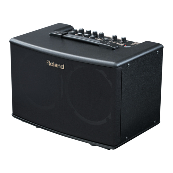
Page 4: Location Of Controls
Jul. 2013 AC-40 Location of Controls fig.panel.eps... -
Page 5: Location Of Controls Parts List
Jul. 2013 AC-40 Location of Controls Parts List Part Code Part Name Description Q’ty 13449146 6.5MM JACK YKB21-5012 (W/SW) 22150756 JACK NUT 2 PLASTIC/BLK 5100011024 R-KNOB(SD000083) 08203-500(40A-KAC-60-B) 5100033257 ROTARY POTENTIOMETER R0923NOCH1P104FD20B4 * This unit includes the following parts. ******** VR NUT M9... -
Page 6: Exploded View (All)
Jul. 2013 AC-40 Exploded View (All) fig.bunkai-all.eps Refer to Fig.A BLACK ORANGE BROWN (#5100033172) (#5100033173) (#5100033174) (#5100033175) *Terminals are on the inside. -
Page 7: Exploded View (All) Parts List
Jul. 2013 AC-40 Exploded View (All) Parts List Part Code Part Name Description Q’ty 5100033223 CABINET ASSY * This unit includes the following parts. 5100006069 RUBBER FOOT(430-BG-435) D25XT18 40484-512(SD001005) 5100009863 STAND HOLDER(40E-1BG-435) 40484-518 (#SD001007) 5100009860 STAND 08203-016 (#SD001169) 5100023934 CATCH D17.5... -
Page 8: Plane View (1)
Jul. 2013 AC-40 Plane View (1) fig.heimen1.eps View 1 View 2 Plane View (1) Parts List View 1 Part Code Part Name Description Q’ty 40237101 SCREW M3X8 PAN MACHINE W/SW+SMALL PW BZC 40010667 SCREW 4X16 TRUSS TAPPING A FE BZC... -
Page 9: Plane View (2)
Jul. 2013 AC-40 Plane View (2) fig.heimen2.eps View 3 View 4 Plane View (2) Parts List View 3 Part Code Part Name Description Q’ty 40010367 SCREW M4X25 BINDING MACHINE BZC View 4 Part Code Part Name Description Q’ty 40012501 SCREW 4X12... -
Page 10: Exploded View (Fig. A)
Jul. 2013 AC-40 Exploded View (Fig. A) fig.bunkai-A-e.eps Solder 2 locations (wound) Solder * The end of the wire must not extend 2 locations below the connector. (wound) Wind the wiring (#5100033167) around the power switch and solder. 20 – 25mm Secure the wiring in place using a clamp. -
Page 11: Exploded View (Fig. A) Parts List
Jul. 2013 AC-40 Exploded View (Fig. A) Parts List Part Code Part Name Description Q’ty 22150756 JACK NUT 2 PLASTIC/BLK 5100011024 R-KNOB(SD000083) 08203-500(40A-KAC-60-B) ******** VR NUT M9 attached to potentiometer ******** VR MASHER attached to potentiometer 02897801 SEESAW SWITCH SDDJE13200 94V-0... -
Page 12: Plane View (Fig. A)
Jul. 2013 AC-40 Plane View (Fig. A) fig.heimenA.eps View A1 View A2 View A3... -
Page 13: Plane View (Fig. A) Parts List
Jul. 2013 AC-40 Plane View (Fig. A) Parts List View A1 Part Code Part Name Description Q’ty 40012867 SCREW M3X8 PAN MACHINE W/SW+PW ZC View A2 Part Code Part Name Description Q’ty 40012867 SCREW M3X8 PAN MACHINE W/SW+PW ZC View A3... -
Page 14: Application Sites For Eva Packing Cushions
Jul. 2013 AC-40 Application Sites for EVA Packing Cushions Mic Input Board Panel Board Give attention to the following point when affixing the EVA Packing Give attention to the following point when affixing the EVA Packing (#5100011617) onto the MIC/LINE CHANNEL INPUT jack. - Page 15 Jul. 2013 AC-40...
-
Page 16: Parts List
Jul. 2013 AC-40 Parts List fig.-part1-e.eps Due to one or more of the following reasons, Safety Precautions: parts with parts code ******** cannot be supplied as service parts. The parts marked have safety-related characteristics. Use only listed parts for replacement. - Page 17 Jul. 2013 AC-40 WIRING, CABLE 5100033165 WIRING W1 5100033166 WIRING W2 5100033167 WIRING W3 5100033168 WIRING W4 5100033169 WIRING W5 5100033170 WIRING W6 5100033171 WIRING W7 5100033172 WIRING W8 5100033173 WIRING W9 5100033174 WIRING W10 5100033175 WIRING W11 5100033176 WIRING W12...
-
Page 18: Verifying The Version
Jul. 2013 AC-40 Verifying the Version Test Mode Items Required Items Required • Foot switch (FS-5U x 2 or FS-6 x 1) • Foot switch (FS-5U x 2 or FS-6 x 1) • Foot-switch connection cable (PCS-31 or PCS-33) * Set the POLARITY switch and the MODE switch on the foot switch as shown •... -
Page 19: Input/Output Level Test (For Reference)
Jul. 2013 AC-40 3. Volume Check Speaker Output Verification Connect a 4 Ω load resistor to the speaker lines. Working in the sequence shown below, change the settings of the controls from minimum to intermediate and to maximum and vice versa, Connect the signal generator to the MIC/LINE CHANNEL INPUT jack and and verify that the LEDs light up and the speaker plays sound. -
Page 20: Wiring Diagram/Block Diagram
Jul. 2013 AC-40 Wiring Diagram/Block Diagram fig.block.eps@L... - Page 21 Jul. 2013 AC-40 fig.block.eps@R Part Code Part Name Description Q’ty 5100033168 WIRING W4 5100033170 WIRING W6 5100033172 WIRING W8 5100033173 WIRING W9 5100033174 WIRING W10 5100033175 WIRING W11 5100033169 WIRING W5 5100033165 WIRING W1 5100033171 WIRING W7 5100033176 WIRING W12...
-
Page 22: Circuit Board (Main Board)
Jul. 2013 AC-40 Circuit Board (Main Board) fig.b-main1.eps... - Page 23 Jul. 2013 AC-40 fig.b-main2.eps...
-
Page 24: Circuit Diagram (Main Board: 1/3)
Jul. 2013 AC-40 Circuit Diagram (Main Board: 1/3) fig.d-main1.eps@L TC7W08FU(TE12L.F) D+3.3V D+3.3V D+3.3V D+3.3V FOR UPDATE EEPROM+3.3V B6B-PH-K-S (LF)(SN) D+3.3V DGND DGND DGND DGND 4.7k 1005 4.7k 1005 4.7k 1005 0.1uF R205 IC19 R206 DGND M24M01-HRMN6TP R207 DGND R208 DGND D+3.3V... - Page 25 Jul. 2013 AC-40 fig.d-main1.eps@R D+3.3V 1005 D+3.3V WP_EEPROM RESET RESET D+3.3V TC7W08FU(TE12L.F) 0.1uF TC7W08FU(TE12L.F) 0.1uF DGND DGND D+1.5V D+3.3V R125 10uF DGND 1005 MUTE_CONTROL DGND D+3.3V CONT_POWEROFF C316 R345 0.1uF UnPop UnPop UnPop R316 POWER_MANAGE DGND R344 D+3.3V UnPop POWER_SW_SENSE...
-
Page 26: Circuit Diagram (Main Board: 2/3)
Jul. 2013 AC-40 Circuit Diagram (Main Board: 2/3) fig.d-main2.eps@L A+3.3V UnPop ELL6SH2R7M LOUT 10uF D+3.3V C100 10V 10uF 16V A+3.3V 2.7uH ROUT 0.1uF 0.1uF AGND R152 SDTI SDTO C237 AGND 100uF LRCK VCOM 2012 MCLK BCLK DEM1 AGND DEMO A+10V AK4552VTP-E2 5.6k... - Page 27 Jul. 2013 AC-40 fig.d-main2.eps@R C179 C177 10uF 16V 2.2k 47pF R110 R103 AGND 8.2k C183 UnPop 100uF 16V 1/2W R101 C176 C190 R116 C181 10uF 16V 10uF 16V IC16 FROM JACK BOARD CN204 R105 NJM4580M(TE2) R328 LINE_MUTE L15 BLM21AG102SN1D 390k...
-
Page 28: Circuit Diagram (Main Board: 3/3)
Jul. 2013 AC-40 Circuit Diagram (Main Board: 3/3) fig.d-main3.eps@L TO POWER SW B2P3S-VH (LF)(SN) 7A/250V CN11 UnPop RSX501L-20TE25 FROM JACK BOARD CN200, CN201 D301 TPC8127 R304 R146 CN23 R305 R145 B2P3S-VH (LF)(SN) 7A/250V C214 100k DGND 470k 0.47uF R147 TPC8127 Q300 2SA1586-GR(TE85R.F) - Page 29 Jul. 2013 AC-40 fig.d-main3.eps@R This area is UnPop PVDD+12V A+10V F300 MRT80 2SC4116-GR(TE85R.F) 2SA1586-GR(TE85R.F) R136 2.2k C216 220uF C215 220uF C218 C313 Q301 C222 0.1uF 470uF DGND Low-ESR UDZS TE-17 10B D+3.3V AGND UnPop R315 2SC4116-GR(TE85R.F) R330 UnPop R341 2SC4116-GR(TE85R.F)
-
Page 30: Circuit Board (Gt Input, Panel, Jack, Mic Input Board)
Jul. 2013 AC-40 Circuit Board (GT Input, Panel, Jack, Mic Input Board) fig.b-panel.eps... -
Page 31: Circuit Diagram (Gt Input Board)
Jul. 2013 AC-40 Circuit Diagram (GT Input Board) fig.d-GT-lnput.eps VA_GT+10V L302 EXCELDR35V D301 1N4148-34 T/B C306 D300 AGND_GTIN L300 R300 0.1uF 1N4148-34 T/B VA_GT+10V Q300 DUMMY-JP05 2SK2881-T112-E C301 Dummy VR300 100kB GUITAR INPUT VA_GT+10V R306 R0923NOCH1P104FD20B4 R313 JK301 C300 R301... -
Page 32: Circuit Diagram (Panel Board)
Jul. 2013 AC-40 Circuit Diagram (Panel Board) fig.d-panel.eps@L REF+3.3V_PANEL SS71020F-0103-6T-025-NP-017 SW3,SW4 REF+3.3V_PANEL WIDE SPACE 10uF 0.1uF 7mm height type REF+3.3V_PANEL REF+3.3V_PANEL VOL05 VR1 10kB VR2 10kB VOL04 VOL03 VOL01 VOL02 VOL02 REF+3.3V_PANEL UnPop UnPop 12P-SAN 0.1uF 2COM SWI3 SWI4 SWI5... - Page 33 Jul. 2013 AC-40 fig.d-panel.eps@R REF+3.3V_PANEL SS71020F-0103-6T-025-NP-017 SWI4 REF+3.3V_PANEL ANTI-FBK ON SWI5 SS71010F-0102-6T-015-NP ANTI-FBK OFF REF+3.3V_PANEL REF+3.3V_PANEL REF+3.3V_PANEL VR4 10kB VR3 10kB VR5 10kB VOL04 VOL03 VOL05 UnPop UnPop UnPop BASS CHORUS REVERB MASTER REF+3.3V_PANEL REF+3.3V_PANEL VR8 10kB VR9 10kB VOL08...
-
Page 34: Circuit Diagram (Jack Board)
Jul. 2013 AC-40 Circuit Diagram (Jack Board) fig.d-jack.eps@L C202 VR200 10uF C219 R1131GOXH1B203TG0027 0.1uF C200 220pF DGND_JK Dummy C201 C203 L202 DUMMY-JP05 R202 220pF 10uF VR200 AUX IN (MINI ) Dummy L203 DUMMY-JP05 R203 JK201 HTJ-035-09ABT C213 0.1uF VR200 R1131GOXH1B203TG0027... - Page 35 Jul. 2013 AC-40 fig.d-jack.eps@R To MAIN BOARD CN9 AUX_IN_L AUX_IN_R AUX_GND LINE_OUT_GND LINE_OUT_L LINE_OUT_R CN202 6P-SAN to MAIN BOARD CN6 L209 DUMMY-JP05 Dummy PHONES_L Dummy PHONES PHONES_R PHONES_GND L207 DUMMY-JP05 PHONES_SENSE CN204 JK202 S5B-PH-K-S (LF)(SN) YKB21-5401N C210 C214 C215 0.1uF...
-
Page 36: Circuit Diagram (Mic Input Board)
Jul. 2013 AC-40 Circuit Diagram (Mic Input Board) fig.d-MIC-lnput.eps@L JK402 CT/PJ-02-EP V_MC+10V D402 1N4148-34 T/B D403 R400 FGND_MC 1N4148-34 T/B C413 Dummy 180pF L401 C402 DUMMY-JP05 C400 10uF R415 1000pF R401 R405 C415 AGND_MC AGND_MC C403 220pF V_MC+10V IC400 220pF... - Page 37 Jul. 2013 AC-40 fig.d-MIC-lnput.eps@R C412 VR400 100kB 0.47uF R417 R0923NOCH1P104FD20B4 2.2k Dummy L402 C416 DUMMY-JP05 R407 V_MC+10V To MAIN BOARD CN7 R419 100k IC400 NJM4580D A+10V C417 CH2_SIG V_MC+1_2V AGND 10uF C423 CN400 B3B-PH-K-S (LF)(SN) V_MC+10V 0.1uF FGND_MC AGND_MC V_MC+1_2V...
Need help?
Do you have a question about the AC-40 and is the answer not in the manual?
Questions and answers