
Summary of Contents for Dwin T5L ASIC Series
- Page 1 DWIN Technology T5L_ASIC Development Guide Professional, Creditable, Successful T5L_ASIC Development Guide Version 2.0 2022/4/13 www.dwin-global.com - 1 -...
-
Page 2: Table Of Contents
DWIN Technology T5L_ASIC Development Guide Professional, Creditable, Successful Contents 1 Summary ............................3 2 Hardware Description........................5 2.1 PIN Definition ..........................5 2.2 Packaging Dimension ........................10 2.3 Basic Performance Parameters ....................11 2.4 Notices for Hardware Design ....................... 12 3 OS CPU ............................ -
Page 3: Summary
➢ Support DGUS development and simulation on PC. Support background remote upgrade. (3) Separated CPU (OS CPU) core runs user 8051 code or DWIN OS system, user CPU omitted in practical application. www.dwin-global.com... - Page 4 (7) Support SD interface or UART1 download and configuration. Support SD card file reading and rewriting. (8) Support DWIN WiFi module to access to DWIN cloud directly, and easily development for various cloud platform applications. (9) Working temperature ranges from - 40℃ to +85℃ (Customizable IC for -55℃ to 105℃...
-
Page 5: Hardware Description
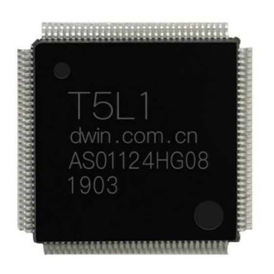
DWIN Technology T5L_ASIC Development Guide Professional, Creditable, Successful 2 Hardware Description 2.1 PIN Definition T5L ASIC is packaged in ELQFP128 (16*16*1.5mm), and pins arrangement are shown below. T5L pin Definition CPU PIN# Function 1 Instructions Function 2 Instructions Function 3... - Page 6 DWIN Technology T5L_ASIC Development Guide Professional, Creditable, Successful P1.0 I/O port P1.1 I/O port P1.2 I/O port P1.3 I/O port P1.4 I/O port P1.5 I/O port P1.6 I/O port P1.7 I/O port T5L1=1.25V T5L2=1.2V 3.3V P2.0 I/O port P2.1 I/O port P2.2...
- Page 7 DWIN Technology T5L_ASIC Development Guide Professional, Creditable, Successful P0.7 I/O port FSK_RX FSK transceiver data receiving 4-wire resistance touch screen ADC0 AD input RTP_X0 interface 4-wire resistance touch screen ADC1 AD input RTP_Y0 interface 4-wire resistance touch screen ADC2 AD input...
- Page 8 DWIN Technology T5L_ASIC Development Guide Professional, Creditable, Successful P2.2 I/O port SPI_CS SPI Flash interface: chip selection P2.3 I/O port SPI_CLK SPI Flash interface: clock Capacitance 4-wire resistance touch screen P2.4 I/O port RTP_Y1 CTP_SDA touch screen interface interface Capacitance 4-wire resistance touch screen P2.5...
- Page 9 DWIN Technology T5L_ASIC Development Guide Professional, Creditable, Successful P5.3 I/O port LCD_G3 LCD interface P5.4 I/O port LCD_G4 LCD interface P5.5 I/O port LCD_G5 LCD interface P5.6 I/O port LCD_G6 LCD interface P5.7 I/O port LCD_G7 LCD interface T5L1=1.25V T5L2=1.2V 3.3V...
-
Page 10: Packaging Dimension
DWIN Technology T5L_ASIC Development Guide Professional, Creditable, Successful 2.2 Packaging Dimension For PCB design, please refer to the DWIN official device packaging and reference design. www.dwin-global.com - 10... -
Page 11: Basic Performance Parameters
DWIN Technology T5L_ASIC Development Guide Professional, Creditable, Successful 2.3 Basic Performance Parameters Parameter Unit Minimum Typical value Maximum Instructions 1.10 1.20 1.30 T5L2 CPU core voltage 1.20 1.25 1.35 T5L1 Dual-core 200MHz full speed CPU core current operation 5V TTL/CMOS level input... -
Page 12: Notices For Hardware Design
DWIN Technology T5L_ASIC Development Guide Professional, Creditable, Successful 2.4 Notices for Hardware Design (1) The core power voltage must be stable, otherwise it will lead to abnormal CPU operation. (2) Reset is recommended to be handled by a low-level reset IC like SGM809S, instead of a simple RC reset circuit. -
Page 13: Os Cpu
The T5L OS CPU adopt the 8051 kernel, which is the most widely used in industry and has longest history in mass production. On the basis of the good real-time performance, fast IO rate and stable reliability of 8051, DWIN has significantly improved the 8051 memory by optimizing the code processing, expanding the SFR bus and enhancing the hardware math processor. -
Page 14: Initial Configuration
DWIN Technology T5L_ASIC Development Guide Professional, Creditable, Successful 3.1 Initial Configuration When the 8051 kernel is powered on, the special function register (SFR) in the following table must be initialized correctly. SFR name Address Initial values Instructions CKON 0X8E 0X00 CPU runs in 1T mode Configure extended interrupt system;... -
Page 15: Memory
8051. Data register 256Bytes 0x00-0xFF The same as standard 8051 The same as standard 8051. DWIN can provide user SFR SFR register 128Bytes 0X80-0XFF definition files( .INC or .H header file). Accessible using the SFR register interface defined by EXADR,... -
Page 16: Variable Memory(256Kbytes)
DWIN Technology T5L_ASIC Development Guide Professional, Creditable, Successful 3.2.2 Variable Memory(256KBytes) (1) 0x00:0000-0x00:7FFF addresses correspond to the 128Kbytes variable memory space currently used by the DGUS II system. For example, the two DGUS II variable memories, 0x1000 and 0x1001, correspond to the 0x0800 address of the OS 8051 DGUS variable memory, where D3 corresponds to the 0x1000 variable high byte and D2 corresponds to the 0x1000 variable low byte;... - Page 17 DWIN Technology T5L_ASIC Development Guide Professional, Creditable, Successful Example Read and write two double words in 0x0800 address (corresponding to DGUSII variable memory address 0x1000). ADR_H,#00H ;Configure DGUS variable memory address ADR_M,#08H ADR_L,#00H ADR_INC,#01H ;Configuration address increment RAMMODE,#0AFH ;Start read mode APP_ACK,$ ;Waiting for confirmation...
-
Page 18: Data Memory(32Kbytes)
DWIN Technology T5L_ASIC Development Guide Professional, Creditable, Successful 3.2.3 Data Memory(32KBytes) The OS 8051 CPU of T5L has 32KBytes RAM as data memory, corresponding to addresses 0x8000- 0xFFFF, and the related interface SFRs are listed below. SFR name Address Instructions DPTR change mode after MOVX instruction operation. -
Page 19: Extended Sfr Register
DWIN Technology T5L_ASIC Development Guide Professional, Creditable, Successful 3.2.4 Extended SFR Register Extended SFR registers use EXADR, EXDDATA register to read and write. SFR name Address Instruction 0xFE Extend the SFR address and automatically add 1 to the next SFR after each reading and writing. -
Page 20: Mathematical Operating Unit(Mdu)
DWIN Technology T5L_ASIC Development Guide Professional, Creditable, Successful 3.3 Mathematical Operating Unit(MDU) Due to the limited computing power of 8051, the hardware mathematic unit (MDU) is extended in T5L to improve computing power. OS 8051 applications can access hardware MAC and hardware divider. - Page 21 DWIN Technology T5L_ASIC Development Guide Professional, Creditable, Successful R6,EXDATA R5,EXDATA R4,EXDATA R3,EXDATA R2,EXDATA R1,EXDATA R0,EXDATA www.dwin-global.com - 21...
-
Page 22: Timer
DWIN Technology T5L_ASIC Development Guide Professional, Creditable, Successful 3.4 Timer T5L OS 8051 has three timers: T0/T1/T2, of which T0/T1 are consistent with standard 8051, and T2 can only work in 16 bit autoload mode. The clocks of T0 and T1 are 1/12 of the CPU main frequency. The clocks of T2 can be configured as 1/12 or 1/24 of the CPU main frequency. - Page 23 DWIN Technology T5L_ASIC Development Guide Professional, Creditable, Successful Example In 11.0592 MHz crystal (corresponding to the main frequency of CPU 206.4384 MHz), T2 1mS interruption is set to output 500 MHz square wave at P 1.0. 002BH ;T2 interrupt program entry...
-
Page 24: Watchdog Timer(Wdt)
DWIN Technology T5L_ASIC Development Guide Professional, Creditable, Successful 3.5 Watchdog Timer(WDT) In order to monitor the operation of the software and ensure that that a system reset is automatically generated to restore normalcy in the event of an abnormality, T5L OS 8051 is equipped with a software watchdog (WDT) timer whose counting reset time is set to 1 second (corresponding to 11.0592 MHz crystal). - Page 25 DWIN Technology T5L_ASIC Development Guide Professional, Creditable, Successful 3.6 IO T5L OS 8051 has three 8 bit parallel ports(P0-P2) and a 4 bit parallel port(P3.0-P3.3), a total of 28 IO ports. P0-P0.7 of P0 port is multiplexed with UART and CAN interface, and multiplexing function or IO function can be selected through MUX_SEL register.
- Page 26 DWIN Technology T5L_ASIC Development Guide Professional, Creditable, Successful Selection of peripheral reuse. .7 1 = CAN interface leads to P 0.2 and P 0.3; 0 = CAN interface is not lead out, and it works as an IO port. .6 1 = UART2 interface leads to P 0.4 and P 0.5; 0 = UART2 interface is not lead out, and it works as an IO port.
-
Page 27: Uart
DWIN Technology T5L_ASIC Development Guide Professional, Creditable, Successful 3.7 UART 3.7.1 UART2 UART2 related SFR are shown in the following table. SFR name Address Instructions .6 1 = UART2 interface leads to P 0.4 and P 0.5; MUX_SEL 0xC9 0 = UART02 interface does not lead out, it works as an IO port . -
Page 28: Uart3
DWIN Technology T5L_ASIC Development Guide Professional, Creditable, Successful 3.7.2 UART3 UART3 related SFRs are shown in the following table. SFR name Address Instructions MUX_SEL 0xC9 .5 1 = UART3 interface leads to P 0.6, P 0.7, 0 = UART3 interface does not lead out, it is IO port. -
Page 29: Uart4
DWIN Technology T5L_ASIC Development Guide Professional, Creditable, Successful 3.7.3 UART4 UART4 related SFR are shown in the following table. SFR name Address Instructions UART4 sending control: .7 UART4 sending enable. 0=close;1=open; .6 0=8bit mode,1=9bit mode; SCON2T 0x96 .5 TB8, 9 th bit sent in 9bit mode;... -
Page 30: Uart5
DWIN Technology T5L_ASIC Development Guide Professional, Creditable, Successful 3.7.4 UART5 The relevant settings of UART5 are as follows: SFR name Address Instructions UART5 sending control: .7 UART5 sending enables. 0=close;1=open; .6 0=8bit mode,1=9bit mode; SCON3T 0xA7 .5 TB8, 9 th bit sent in 9bit mode;... -
Page 31: Can
DWIN Technology T5L_ASIC Development Guide Professional, Creditable, Successful 3.8 CAN The SFRs associated with the CAN interface are shown in the following table : SFR name Address Instructions .7 1 = CAN interface leads to P 0.4 and P 0.5,0 = CAN interface does not lead out, it is IO port . - Page 32 DWIN Technology T5L_ASIC Development Guide Professional, Creditable, Successful 0xFF:0062 D3:D0 AMR3:0 Acceptance code register RXERR Receiving error count register 0xFF:0063 TXERR Sending error count register D1:D0 Undefined Write 0 CAN_TX_B [7]IDE,[6]RTR,[3:0]—DLC, frame data length UFFER 0xFF:0064 D2:D0 Undefined ID, 29bit is valid for extended frame and 11bit is valid for standard frame.
-
Page 33: Interrupt System
DWIN Technology T5L_ASIC Development Guide Professional, Creditable, Successful 3.9 Interrupt System 3.9.1Interrupt Control SFR T5L OS CPU has 12 interrupts. The related control SFRs list is as follows: Address Instructions name The interrupt enable controller 0 can be addressed by bit. -
Page 34: Interrupt Priority
DWIN Technology T5L_ASIC Development Guide Professional, Creditable, Successful 3.9.2 Interrupt Priority The interrupt priority of T5L OS CPU is handled according to the following rules. (1) Twelve interrupts are divided into six groups with two interrupts in each group. The priority in the same group is fixed. - Page 35 DWIN Technology T5L_ASIC Development Guide Professional, Creditable, Successful Note The T5L OS CPU is fast (1uS can execute 130-150 instructions on average) and the interrupt execution time is short, so the real-time performance is already very high. It is not recommended to use interrupt embedding that makes program architecture more complex.
-
Page 36: T5L Asic 8051 Instruction Set
DWIN Technology T5L_ASIC Development Guide Professional, Creditable, Successful 3.10 T5L ASIC 8051 Instruction Set Instruction Instruction Instruction Instruction Instruction format Instruction format length cycle length cycle ADD/ADDDC A,Rn MOV @Ri,direct ADD/ADDDC A,direct MOV @Ri,#data ADD/ADDDC A,@Ri MOV DPTR,#data16 ADD/ADDDC A,@data... - Page 37 DWIN Technology T5L_ASIC Development Guide Professional, Creditable, Successful MOV @Ri,A MOV bit,C CPU main frequency = crystal frequency * 56/3. 11.0592MHz crystal corresponds to 206.438MHz main frequency, corresponding to an instruction cycle (1T) of 4.844nS. Example Under 11.0592 MHz crystal, the following code will output 206.4384/((2+2)*2)=25.8048 MHz square wave on the P3.3 IO interface.
-
Page 38: Simulation Debug
After installation, copy the header file of T5L OS CPU (*. INC or *. h) to KEIL/C51/INC/DWIN directory. (3) Before setting the breakpoint to read the content of data storage (XDATA), DPC = 0x00 must be ensured, otherwise the data will be misaligned. - Page 39 Optimize the algorithm of the original code with MDU hardware computing acceleration; move the UI and Internet (e.g., access to DWIN cloud through DWIN WiFi module) functions to DGUS II platform, user code can be processed by simply reading and writing DGUS variable space, which can significantly improve product performance and enhance R&D efficiency.
-
Page 40: Ek043 Evaluation Board
(5) Read and write DGUS variable memory and download pictures and word libraries through USB interface to facilitate DGUS debugging; (6) The assembly location of DWIN WiFi module is reserved for easy access to DWIN cloud (both WiFi module and USB occupy the UART with a baud rate of 921600 bps);... - Page 41 T5L_ASIC Development Guide Professional, Creditable, Successful If you have any questions during the use of this document or DWIN products, or want to know more about the latest information of DWIN products, please contact us. Hotline: 400 018 9008 Whatsapp: + 8619192113166 DWIN website: https://www.dwin-global.com/...
Need help?
Do you have a question about the T5L ASIC Series and is the answer not in the manual?
Questions and answers