Table of Contents
Advertisement
Quick Links
SERVICE MANUAL
Ver. 1.0 2010.07
• The tuner and CD sections have no adjustments.
Tuner section
FM
Tuning range:
87.5 – 107.9 MHz
Antenna (aerial) terminal:
External antenna (aerial) connector
Intermediate frequency: 150 kHz
Usable sensitivity: 10 dBf
Selectivity: 75 dB at 400 kHz
Signal-to-noise ratio: 70 dB (mono)
Separation: 40 dB at 1 kHz
Frequency response: 20 – 15,000 Hz
AM
Tuning range:
530 – 1,710 kHz
Antenna (aerial) terminal:
External antenna (aerial) connector
Intermediate frequency: 25 kHz
Sensitivity: 26 μV
Sony Corporation
9-889-900-01
2010G04-1
Audio&Video Business Group
©
2010.07
Published by Sony Techno Create Corporation
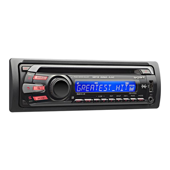
CDX-GT35UW
Model Name Using Similar Mechanism
CD Drive Mechanism Type
Optical Pick-up Name
SPECIFICATIONS
CD player section
Signal-to-noise ratio: 120 dB
Frequency response: 10 – 20,000 Hz
Wow and fl utter: Below measurable limit
USB Player section
Interface: USB (Full-speed)
Maximum current: 500 mA
Power amplifi er section
Outputs: Speaker outputs
Speaker impedance: 4 – 8 ohms
Maximum power output:
52 W × 4 (at 4 ohms)
General
Outputs:
Audio outputs terminal
(sub/rear switchable)
Power antenna (aerial) relay control terminal
Power amplifi er control terminal
FM/AM COMPACT DISC PLAYER
US Model
CDX-GT33U
MG-101Y-188//Q
DAX-25A
Inputs:
Antenna (aerial) input terminal
AUX input jack (stereo mini jack)
USB signal input connector
Tone controls:
Low: ±10 dB at 60 Hz (XPLOD)
Mid: ±10 dB at 1 kHz (XPLOD)
High: ±10 dB at 10 kHz (XPLOD)
Power requirements: 12 V DC car battery
(negative ground (earth))
Dimensions: Approx. 178 × 50 × 179 mm
(7
1
/
× 2 × 7
1
/
in.) (w/h/d)
8
8
Mounting dimensions:
Approx. 182 × 53 × 162 mm
(7
1
/
× 2
1
/
× 6
1
/
in.) (w/h/d)
4
8
2
– Continued on next page –
Advertisement
Table of Contents

Related Manuals for Sony CDX-GT35UW


Summary of Contents for Sony CDX-GT35UW
- Page 1 – Continued on next page – Intermediate frequency: 25 kHz (sub/rear switchable) Sensitivity: 26 μV Power antenna (aerial) relay control terminal Power amplifi er control terminal FM/AM COMPACT DISC PLAYER Sony Corporation 9-889-900-01 2010G04-1 Audio&Video Business Group © 2010.07 Published by Sony Techno Create Corporation...
- Page 2 COMPONENTS IDENTIFIED BY MARK 0 OR DOTTED LINE WITH MARK 0 ON THE SCHEMATIC DIAGRAMS AND IN THE PARTS LIST ARE CRITICAL TO SAFE OPERATION. REPLACE THESE COMPONENTS WITH SONY PARTS WHOSE PART NUMBERS APPEAR AS SHOWN IN THIS MANUAL OR IN SUPPLEMENTS PUBLISHED BY SONY.
-
Page 3: Table Of Contents
CDX-GT35UW UNLEADED SOLDER TABLE OF CONTENTS Boards requiring use of unleaded solder are printed with the lead- free mark (LF) indicating the solder contains no lead. SERVICE NOTE ............(Caution: Some printed circuit boards may not come printed with the lead free mark due to their particular size) GENERAL Connections .............. -
Page 4: Service Note
CDX-GT35UW SECTION 1 SERVICE NOTE EXTENSION CABLE AND SERVICE POSITION When repairing or servicing this set, connect the jig (extension cable) as shown below. • Connect the MAIN board (CN701) and the SERVO board (CN401) with the extension cable (Part No. J-2502-076-1). -
Page 5: General
CDX-GT35UW SECTION 2 GENERAL This section is extracted from instruction manual. • CONNECTIONS... -
Page 6: Disassembly
CDX-GT35UW SECTION 3 DISASSEMBLY • This set can be disassembled in the order shown below. 3-1. SUB PANEL ASSY (Page 7) 3-2. CD MECHANISM BLOCK (Page 7) 3-4. SERVO BOARD 3-3. MAIN BOARD (Page 8) (Page 8) 3-5. CHASSIS (T) SUB ASSY (Page 9) 3-6. -
Page 7: Sub Panel Assy
CDX-GT35UW Note: Follow the disassembly procedure in the numerical order given. 3-1. SUB PANEL ASSY two claws two claws two screws (+PTT 2.6 × 6) sub panel assy 3-2. CD MECHANISM BLOCK 7 bracket (CD) 8 CD mechanism block 6 two screws (+PTT 2.6... -
Page 8: Main Board
CDX-GT35UW 3-3. MAIN BOARD 2 two screws (+PTT 2.6 4 two screws (+P 2.6 5 two screws (+PTT 2.6 1 three screws 6 screw (+BTT 2.6 5.2) (+P 2.6 7 screw (+PTT 2.6 8 heat sink 9 MAIN board insulating sheet 3-4. -
Page 9: Chassis (T) Sub Assy
CDX-GT35UW 3-5. CHASSIS (T) SUB ASSY 2 two screws 1 two screws (M 1.7 2.5) (M 1.7 2.5) 4 chassis (T) sub assy 3 claw 3-6. ROLLER ARM ASSY 6 roller arm assy 4 gear (RA1) 1 spring (RAL) 3 washer... -
Page 10: Chassis (Op) Assy
CDX-GT35UW 3-7. CHASSIS (OP) ASSY 6 chassis (OP) assy 1 tension spring (KF) 7 two coil springs (damper) (natural) 8 coil spring (damper) (green) 4 slider (R) 3 lever (D) 2 gear (LE1) 3-8. CHUCKING ARM SUB ASSY 3 chucking arm sub assy 1 spring Note: Have this portion receive the chassis. -
Page 11: Sled Motor Assy
CDX-GT35UW 3-9. SLED MOTOR ASSY 2 three serration screws (M 2 3 sled motor assy 1 spring turn table spring stand Note: Never remove these parts since they were adjusted. bearing (F) stand Note: Place the stand with care not to touch the turn table. -
Page 12: 3-10. Optical Pick-Up Section
CDX-GT35UW 3-10. OPTICAL PICK-UP SECTION 2 optical pick-up section Note: Be careful not to touch the lens and hologram terminal when removing the optical pick-up section. 3-11. OPTICAL PICK-UP 1 tapping screw (P 1.4) 2 leaf spring (OPS) 3 rack... -
Page 13: Diagrams
CDX-GT35UW SECTION 4 DIAGRAMS 4-1. BLOCK DIAGRAM – MAIN Section – ELECTRONIC VOLUME IC804 J303 AUDIO O/P SUB L REAR/SUB O/P SUB R R-CH (REAR/SUB) R-CH R-CH J901 I2C BUS CONTROLLED 7 AUX-LCH ZAP BEEP R POWER AMP/MULTIPLE R-CH 9 AUX-RCH... -
Page 14: Block Diagram -Display Section
CDX-GT35UW 4-2. BLOCK DIAGRAM – DISPLAY Section – SYSTEM CONTROL LCD DRIVER,LED CONTROL IC401 (2/2) IC901 KEY_IN1 KEY MATRIX LCD_SO DATA LSW901 LCD_SCK CLK LCD PANEL+B S902–908 KEY_IN0 LCD_CE SEG48 LCD901 46 KEY_ACK1 LED911,913–915,918, SEG2 LED901 LIQUID 924,925,930,931, SEG52 (LCD BACK LIGHT) CRYSTAL LSW901,905–913... - Page 15 CDX-GT35UW THIS NOTE IS COMMON FOR PRINTED WIRING BOARDS AND SCHEMATIC DIAGRAMS. • Waveforms (In addition to this, the necessary note is printed in each block.) – MAIN Board – For Printed Wiring Boards: For Schematic Diagrams: Note: Note: IC401 qd (X_OUT) •...
-
Page 16: Printed Wiring Board -Main Section
CDX-GT35UW 4-3. PRINTED WIRING BOARD – MAIN Section – • : Uses unleaded solder. J303 AUDIO OUT REAR/SUB (ANTENNA) C115 C215 CN802 R829 C107 C114 C214 C207 C315 C304 JW220 R107 C113 C213 FU601 C305 C810 C405 IC301 R117 R217... -
Page 17: Schematic Diagram -Main Section (1/3)
CDX-GT35UW 4-4. SCHEMATIC DIAGRAM – MAIN Section (1/3) – • See page 22 for IC Block Diagram. MAIN BOARD (1/3) IC301 IC B/D IC301 TDA8588AJ/N2/R1 I2C BUS CONTROLLED POWER AMP/MULTIPLE VOLTAGE REGULATOR CN802 FRONT 14.4 FU601 L-CH L801 REAR L-CH... -
Page 18: Schematic Diagram -Main Section (2/3)
CDX-GT35UW 4-5. SCHEMATIC DIAGRAM – MAIN Section (2/3) – • See page 15 for waveforms. • See page 22 for IC Block Diagrams. • See page 24 for IC Pin Function Description of IC401. MAIN BOARD (Page 17) (1/3) MAIN BOARD (2/3) -
Page 19: Schematic Diagram -Main Section (3/3)
CDX-GT35UW 4-6. SCHEMATIC DIAGRAM – MAIN Section (3/3) – • See page 15 for waveforms. • See page 22 for IC Block Diagrams. J303 MAIN BOARD (3/3) C107 100p J303 C207 REAR/SUB AUDIO OUT 100p C213 C113 100p 100p Q102-104,202-204... -
Page 20: Printed Wiring Boards -Key Section
CDX-GT35UW 4-7. PRINTED WIRING BOARDS – KEY Section – • : Uses unleaded solder. KEY BOARD (SIDE A) LED907 LED907,S907 LSW901 LED911,913, LSW901 S907 S906 SOURCE LED914,S905 S906 S905 R943 R947 LED901 LED915 LCD901 LED915,S908 LIQUID CRYSTAL DISPLAY PANEL S908... -
Page 21: Schematic Diagram -Key Section
CDX-GT35UW 4-8. SCHEMATIC DIAGRAM – KEY Section – KEY BOARD CN901 D912 MAZ8068GMLS0 D911 R935 R907 R905 USB_VBUS MAZ8068GMLS0 IC902 R906 USB_GND IC902 KEY_GND RS-470 REMOTE CONTROL LSW905 USB_D+ LED901 LSW901 R920 SIGNAL RECEIVER AUX_LCH DSPL/SCRL NESW505DT-A0-UV AUX_LCH (LCD BACK LIGHT) - Page 22 CDX-GT35UW • IC Block Diagrams IC301 TDA8588AJ/N2/R1 (MAIN Board (1/3)) IC402 TK11133CSCL-G (MAIN Board (1/3)) IC501 TPS40200DRG4 (MAIN Board (2/3)) UVLO OVERHEAT & OUT-FL– OVERCURRENT C BUS PROTECTION ISNS CONTROL OUT-FL+ CIRCUIT DRIVER OUT-RL– LOGIC P-GND1 BAND GAP E/A AND SS...
- Page 23 CDX-GT35UW IC804 BD3705FV-E2 (MAIN Board (3/3)) I2C BUS LOGIC FADER FADER FADER FADER FADER LOUDNESS 3 BAND P-EQ(TONE CONTROL) VOLUME/MUTE LEVEL METER (I2C) INPUT GAIN INPUT SELECTOR (2 SIGNAL END 2 STEREO (SO)) ISO AMP ISO AMP ISO AMP ISO AMP...
- Page 24 ― UNISI SONY-BUS data input Not used. UNISO SONY-BUS data output Not used. (Open) UNISCK SONY-BUS clock signal output Not used. (Open) USB_ON USB over current detect IC control signal output I2C_SIO I2C serial data input/output I2C_SCK I2C serial clock signal output...
- Page 25 CDX-GT35UW Pin No. Pin Name Description MC_TX MC-BUS communication and CD mechanism deck micon communication TX output CLK_IN Flash programming serial clock signal input Z_MUTE Z mute signal input Not used. (Open) TEST Not used. (Open) Power supply pin (+3.3 V) ―...
-
Page 26: Exploded Views
CDX-GT35UW SECTION 5 EXPLODED VIEWS Note: • -XX and -X mean standardized parts, so • The mechanical parts with no reference The components identifi ed by mark 0 they may have some difference from the number in the exploded views are not sup- or dotted line with mark 0 are critical for original one. -
Page 27: Front Panel Section
CDX-GT35UW 5-2. FRONT PANEL SECTION not supplied (KEY board) RE901 not supplied not supplied (JACK board) not supplied CN902 LCD901 not supplied not supplied not supplied not supplied not supplied Ref. No. Part No. Description Remark Ref. No. Part No. -
Page 28: Cd Mechanism Section (Mg-101Y-188//Q)
CDX-GT35UW 5-3. CD MECHANISM SECTION (MG-101Y-188//Q) not supplied not supplied not supplied not supplied not supplied not supplied not supplied not supplied not supplied not supplied not supplied not supplied Ref. No. Part No. Description Remark Ref. No. Part No. -
Page 29: Electrical Parts List
CDX-GT35UW SECTION 6 JACK ELECTRICAL PARTS LIST Note: • Due to standardization, replacements in • COILS When indicating parts by reference num- the parts list may be different from the uH: μH ber, please include the board name. parts specifi ed in the diagrams or the com- •... - Page 30 CDX-GT35UW MAIN Ref. No. Part No. Description Remark Ref. No. Part No. Description Remark R921 1-216-821-11 METAL CHIP 1/10W VDR903 1-804-988-21 VARISTOR, CHIP (1608) R922 1-216-821-11 METAL CHIP 1/10W VDR906 1-804-988-21 VARISTOR, CHIP (1608) R923 1-216-822-11 METAL CHIP 1.2K 1/10W...
- Page 31 CDX-GT35UW MAIN Ref. No. Part No. Description Remark Ref. No. Part No. Description Remark C217 1-126-964-11 ELECT 10uF C516 1-107-826-11 CERAMIC CHIP 0.1uF C301 1-162-964-11 CERAMIC CHIP 0.001uF C518 1-126-934-11 ELECT 220uF C302 1-162-923-11 CERAMIC CHIP 47PF C519 1-165-908-11 CERAMIC CHIP 1uF...
- Page 32 CDX-GT35UW MAIN Ref. No. Part No. Description Remark Ref. No. Part No. Description Remark D807 6-501-782-01 DIODE MAZ8180GMLS0 JC125 1-216-864-11 SHORT CHIP D809 6-501-782-01 DIODE MAZ8180GMLS0 JC126 1-216-295-91 SHORT CHIP D810 6-501-782-01 DIODE MAZ8180GMLS0 JC127 1-216-295-91 SHORT CHIP D811 6-501-782-01...
- Page 33 CDX-GT35UW MAIN Ref. No. Part No. Description Remark Ref. No. Part No. Description Remark R112 1-216-821-11 METAL CHIP 1/10W R448 1-216-845-11 METAL CHIP 100K 1/10W R113 1-216-833-11 METAL CHIP 1/10W R450 1-216-845-11 METAL CHIP 100K 1/10W R116 1-216-813-11 METAL CHIP...
- Page 34 CDX-GT35UW MAIN SERVO Ref. No. Part No. Description Remark R832 1-216-833-11 METAL CHIP 1/10W R833 1-216-864-11 SHORT CHIP < SWITCH > S401 1-786-826-11 SWITCH, TACTILE (RESET) < SURGE ABSORBER > 1-805-043-11 ABSORBER, CHIP SURGE < VIBRATOR > 1-814-302-11 QUARTZ CRYSTAL UNIT (4MHz)
- Page 35 CDX-GT35UW MEMO...
- Page 36 CDX-GT35UW REVISION HISTORY Checking the version allows you to jump to the revised page. Also, clicking the version at the top of the revised page allows you to jump to the next revised page. Ver. Date Description of Revision 2010.07...