
Related Manuals for Mesa 6i68

Summary of Contents for Mesa 6i68
- Page 1 All manuals and user guides at all-guides.com 6I68 3X2X MOTHERBOARD MANUAL Version 1.3...
- Page 2 All manuals and user guides at all-guides.com This page intentionally not blank...
-
Page 3: Table Of Contents
VIOSELECT ........... 4 6I68 / MODULE PIN CORRESPONDENCE CONNECTORS . -
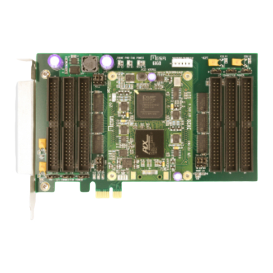
Page 4: General
FPGA daughtercards. The 6I68 breaks out the high density daughterboard I/O connections into six 50 pin .1" headers with standard AnythingIO pinouts. The 6I68 also provides up to 4A of 5V power for I/O connectors via an on card switching regulator. Bus switches are provided on all 144 I/O pins to allow interfacing with 5V I/O. -
Page 5: Hardware Configuration
EEPROM enable function, When W8 is in the up position (default) the EEPROM is enabled. When W8 is in the down position, the EEPROM is disabled. To fix a broken EEPROM setup, you must power up the 6I68 and module card with the EEPROM disabled, Enable the EEPROM, and re-write the EEPROM. -
Page 6: Connector Power
W1 selects the voltage supplied to P5. (I/O connector for bits 120..143) BUS SWITCH MODE The 6I68 uses bus switch devices in series with all I/O pins. These devices allow the 3X2X inputs to be 5V tolerant and allow the I/O pins to be pulled up to 5V. The bus switch input protection function works by disconnecting the FPGA from the IO pins when the IO pin voltage rises above a preset threshold. -
Page 7: Autconfig
The 6I68s’ I/O connectors all end up with 16 I/O pins with selectable VIO and 8 pins with a fixed 3.3VIO on each connector. Note that FPGA configuration used with a 6I68 needs to use the proper ucf file with 6I68 pinouts. These ucf files should have 6I68 or 7I68 in their name. -
Page 8: Connectors
All manuals and user guides at all-guides.com CONNECTORS CONNECTOR LOCATIONS AND DEFAULT JUMPER POSITIONS 6I68 Manual 5... -
Page 9: I/O Connector Pin-Out
LEFT VIO IO15 IO45 LEFT VIO IO16 IO50 FIXED 3.3VIO IO17 IO51 FIXED 3.3VIO IO18 IO56 FIXED 3.3VIO IO19 IO57 FIXED 3.3VIO IO20 IO62 FIXED 3.3VIO IO21 IO63 FIXED 3.3VIO IO22 IO68 FIXED 3.3VIO IO23 IO69 FIXED 3.3VIO 6I68 Manual 6... - Page 10 LEFT VIO IO39 IO47 LEFT VIO IO40 IO52 FIXED 3.3VIO IO41 IO53 FIXED 3.3VIO IO42 IO58 FIXED 3.3VIO IO43 IO59 FIXED 3.3VIO IO44 IO64 FIXED 3.3VIO IO45 IO65 FIXED 3.3VIO IO46 IO70 FIXED 3.3VIO IO47 IO71 FIXED 3.3VIO 6I68 Manual 7...
- Page 11 LEFT VIO IO63 IO43 LEFT VIO IO64 IO48 FIXED 3.3VIO IO65 IO49 FIXED 3.3VIO IO66 IO54 FIXED 3.3VIO IO67 IO55 FIXED 3.3VIO IO68 IO60 FIXED 3.3VIO IO69 IO61 FIXED 3.3VIO IO70 IO66 FIXED 3.3VIO IO71 IO67 FIXED 3.3VIO 6I68 Manual 8...
- Page 12 RIGHT VIO IO87 IO115 RIGHT VIO IO88 IO120 FIXED 3.3VIO IO89 IO121 FIXED 3.3VIO IO90 IO126 FIXED 3.3VIO IO91 IO127 FIXED 3.3VIO IO92 IO132 FIXED 3.3VIO IO93 IO133 FIXED 3.3VIO IO94 IO138 FIXED 3.3VIO IO95 IO139 FIXED 3.3VIO 6I68 Manual 9...
- Page 13 RIGHT VIO IO111 IO117 RIGHT VIO IO112 IO122 FIXED 3.3VIO IO113 IO123 FIXED 3.3VIO IO114 IO128 FIXED 3.3VIO IO115 IO129 FIXED 3.3VIO IO116 IO134 FIXED 3.3VIO IO117 IO135 FIXED 3.3VIO IO118 IO140 FIXED 3.3VIO IO119 IO141 FIXED 3.3VIO 6I68 Manual 10...
- Page 14 RIGHT VIO IO135 IO119 RIGHT VIO IO136 IO124 FIXED 3.3VIO IO137 IO125 FIXED 3.3VIO IO138 IO130 FIXED 3.3VIO IO139 IO131 FIXED 3.3VIO IO140 IO136 FIXED 3.3VIO IO141 IO137 FIXED 3.3VIO IO142 IO142 FIXED 3.3VIO IO143 IO143 FIXED 3.3VIO 6I68 Manual 11...
-
Page 15: Differential Pairs
DIFFERENTIAL PAIRS The 6I68 supports LVDS signaling on all I/O pairs, that is all even/odd I/O pins starting with 0 comprise a differential pair on the 6I68. Which FPGA pins can have LVDS capability depends on the specific daughterboard module. -
Page 16: Operation
The FPGA chips used in the 3X2X modules are not 5V tolerant but external bus switch parts are used on the 6I68 to make the I/O pins 5V tolerant. The bus switch parts disconnect the FPGA pins from the I/O pins when the I/O pins are driven to positive voltage levels that would damage the FPGA. -
Page 17: Reference Information
Per Connector MAX 3.3V CURRENT TO I/O CONNS --- 300 mA Per Connector ABSOLUTE MAX I/O PIN VOLTAGE -.5V 5V tolerant mode ABSOLUTE MAX I/O PIN VOLTAGE -.5V 3.3V mode TEMPERATURE RANGE -C version TEMPERATURE RANGE -I version 6I68 Manual 14...
Need help?
Do you have a question about the 6i68 and is the answer not in the manual?
Questions and answers