Advertisement
Quick Links
COMMUNICATIONS RECEIVER
VR-120D
Technical Supplement
©2002 VERTEX STANDARD CO., LTD. Printed in Japan.
Introduction
This manual provides technical information necessary for
servicing the Yaesu VR-120D Communications Receiver.
Information on its installation and operation can be found
in the VR-120D Operating Manual, which is provided with
the receiver, and Accessory information may be found in
the documents accompanying the optional equipment.
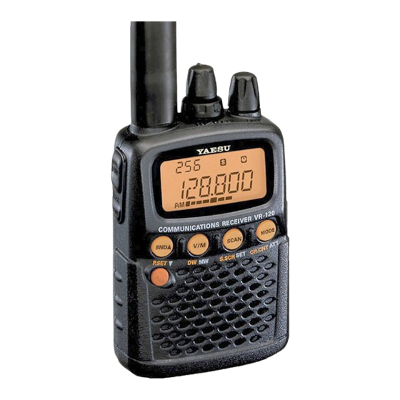
The VR-120D is a high-performance miniature
communications receiver providing general coverage
reception from 100 kHz to 1300 MHz on the AM, and FM
(Wide and Narrow bandwidths) modes (this coverage
includes the AM and FM broadcast bands, HF Short-wave
Bands up to 16 MHz, VHF and UHF TV bands, the VHF
AM aircraft band, and a wide range of commercial and
public safety frequencies!).
Servicing this equipment requires expertise in handling
surface mount chip components. Attempts by unqualified
persons to service this equipment may result in permanent
damage not covered by warranty. For the major circuit
boards, each side of the board is identified by the type of
the majority of components installed on that side. In most
cases one side has only chip components, and the other
has either a mixture of both chip and lead components
(trimmers, coils, electrolytic capacitors, packaged ICs, etc.),
or lead components only.
Specifications ............................................................................................................................................... 2
Exploded View & Miscellaneous Parts ..................................................................................................... 3
Circuit Description ...................................................................................................................................... 5
Alignment ..................................................................................................................................................... 7
Block Diagram .............................................................................................................................................13
Board Unit (Schematics, Layouts & Parts)
AF Unit ........................................................................................................................................................ 15
•
RF Unit .................................................................................................................................................................... 23
All manuals and user guides at all-guides.com
EH011M90A
Contents
VERTEX STANDARD CO., LTD.
4-8-8 Nakameguro, Meguro-Ku, Tokyo 153-8644, Japan
VERTEX STANDARD
US Headquarters
17210 Edwards Rd., Cerritos, CA 90703, U.S.A.
International Division
8350 N.W. 52nd Terrace, Suite 201, Miami, FL 33166, U.S.A.
YAESU EUROPE B.V.
P.O. Box 75525, 1118 ZN Schiphol, The Netherlands
YAESU UK LTD.
Unit 12, Sun Valley Business Park, Winnall Close
Winchester, Hampshire, SO23 0LB, U.K.
VERTEX STANDARD HK LTD.
Unit 5, 20/F., Seaview Centre, 139-141 Hoi Bun Road,
Kwun Tong, Kowloon, Hong Kong
While we believe the technical information in this manual
is correct, VERTEX STANDARD assumes no liability for
damage that may occur as a result of typographical or
other errors that may be present. Your cooperation in
pointing out any inconsistencies in the technical
information would be appreciated. VERTEX STANDARD
reserves the right to make changes in this receiver and the
alignment procedures, in the interest of technological
improvement, without notification of owners.
1
Advertisement

Subscribe to Our Youtube Channel
Related Manuals for Vertex Standard VR-120D

Summary of Contents for Vertex Standard VR-120D
-
Page 1: Table Of Contents
This manual provides technical information necessary for servicing the Yaesu VR-120D Communications Receiver. Information on its installation and operation can be found in the VR-120D Operating Manual, which is provided with the receiver, and Accessory information may be found in the documents accompanying the optional equipment. - Page 2 All manuals and user guides at all-guides.com Alignment Note:...
-
Page 3: Specifications
All manuals and user guides at all-guides.com Specifications Frequency Range: USA: 100 kHz ~ 1299.995 MHz (Cellular Blocked) EXP: 100 kHz ~ 1299.995 MHz (Frequency range is varied per local law. Ask your YAESU dealer for details for frequency range in your country.) Receiving Mode: AM/ FM/ WFM Circuit Type:... -
Page 4: Exploded View & Miscellaneous Parts
All manuals and user guides at all-guides.com Exploded View & Miscellaneous Parts S8001926 BATTERY COVER S8001944 BATTERY PACKING S8001996 REAR CASE À S8001947 S8101008 À CONTACT D BAR ANTENNA ASSY S8001736 Á S8101168 CONTACT B RF Unit S8001939 Á WATER PROOF FILM S8001999 S8001737 FRAME... - Page 5 All manuals and user guides at all-guides.com Exploded View & Miscellaneous Parts Note:...
-
Page 6: Circuit Description
All manuals and user guides at all-guides.com Circuit Description VR-120D separates into two substrate blocks. It is CNTL•AF unit RF unit and CNTL AF unit. • The detected signal from the RF substrate, which is amplified by Q130 (UMX2N), and volume... - Page 7 All manuals and user guides at all-guides.com Circuit Description Note:...
-
Page 8: Alignment
All manuals and user guides at all-guides.com Alignment Introduction Required Test Equipment The VR-120D has been carefully aligned at the The following test equipment (and thorough factory for the specified performance across the familiarity with its correct use) is necessary for amateur band. - Page 9 Set up the test equipment as shown below for r Connect the DC voltmeter to TP3, and referring receiver alignment. to table below, tune the VR-120D to each frequency listed. RF Sinal Generator Then confirm that the correct voltage is present.
- Page 10 All manuals and user guides at all-guides.com Alignment Alignment Points L229 FM Discriminator Adjust VCO VCV: DC voltmeter C305 PLL Reference Frequency Adjust RF Voltege: PLL Reference Frequency Adjust: DC voltmeter Frequency Counter...
- Page 11 All manuals and user guides at all-guides.com Alignment r Tune the receiver to 448.250 MHz. r Increase the SSG output level to 15 dBµ. r Press and hold the [ SCAN ] key for 2 seconds, r Press the [ SCAN ] key while press and holding the rotate the DIAL knob to select the display to [ FUNC ] key.
- Page 12 All manuals and user guides at all-guides.com Alignment r Press the [ BND (p)] key while press and holding AM mode: [ FUNC ] key. " " will appear on the S M ET+ r Set the receiver to 1.050 MHz, AM mode. display.
-
Page 13: Block Diagram
All manuals and user guides at all-guides.com Block Diagram... - Page 14 All manuals and user guides at all-guides.com Block Diagram Note:...
- Page 15 All manuals and user guides at all-guides.com CNTL•AF Unit Circuit Diagram USA B1 B2 R113...
- Page 16 All manuals and user guides at all-guides.com CNTL•AF Unit Note:...
- Page 17 All manuals and user guides at all-guides.com CNTL•AF Unit Parts Layout RN5VL20A (B0) 2SA1588Y (ZY) (Q112) (Q124, 125, 128) UMG2N (G2) UMW1 (W1) (Q113) (Q126, 127) DTA144EE (16) 1SS382 (A1) (Q114) (Q129) XC6371A351PR (A35) UMX2N (X2) (Q116) (Q130) DTC144EE (26) XC6201P322PR (P32) (Q131, 142) (Q118)
- Page 18 All manuals and user guides at all-guides.com CNTL•AF Unit HD6433837SD AT24C64N-10SI1.8SL722A (Q101) (Q115) RB706F-40T106 (3J) 1SS382 (A1) (Q120, 121) (Q102, 103, 104) 2SC4617 (BR) 2SD1615 (GK) (Q107, 110) (Q136) Side B...
-
Page 19: Cntl•Af Unit
All manuals and user guides at all-guides.com CNTL•AF Unit Parts List REF. DESCRIPTION VALUE TOL. MFR’S DESIG VXSTD P/N VERS. LOT. LAY ADR PCB with Component (W/ LCD ASS'Y, SHIELD CASE, CUSHION, CONTACT C) S8101164 PCB with Component (W/ LCD ASS'Y, SHIELD CASE, CUSHION, CONTACT C) S8101165 PCB with Component (W/ LCD ASS'Y, SHIELD CASE, CUSHION, CONTACT C) S8101166... - Page 20 All manuals and user guides at all-guides.com CNTL•AF Unit REF. DESCRIPTION VALUE TOL. MFR’S DESIG VXSTD P/N VERS. LOT. LAY ADR Q116 XC6371A351PR G1093343 Q117 DIODE RB520S-30TE61 G2070822 Q118 XC6201P322PR G1093624 Q120 DIODE RB706F-40T106 G2070824 Q121 DIODE RB706F-40T106 G2070824 Q123 TA31056F(TP1) G1093070 Q124...
- Page 21 All manuals and user guides at all-guides.com CNTL•AF Unit REF. DESCRIPTION VALUE TOL. MFR’S DESIG VXSTD P/N VERS. LOT. LAY ADR R150 CHIP RES. 1/16W RMC1/16 102JATP J24185102 R151 CHIP RES. 1/16W RMC1/16 102JATP J24185102 R152 CHIP RES. 1/16W RMC1/16 102JATP J24185102 R153 CHIP RES.
- Page 22 All manuals and user guides at all-guides.com CNTL•AF Unit Note:...
-
Page 23: Rf Unit
All manuals and user guides at all-guides.com RF Unit Circuit Diagram... - Page 24 All manuals and user guides at all-guides.com RF Unit Note:...
- Page 25 All manuals and user guides at all-guides.com RF Unit Parts Layout 1SS364 (BF) DTA144EE (16) (Q205, 213, 215) (Q225) 2SJ144Y (VY) 2SC5010 (83) (Q227) (Q214) 2SC4915Y (QY) (Q220) 2SC4617R (BR) (Q233) 2SC5006 (24) (Q240, 241) µPC2757T (C1Y) (Q218) Side A...
- Page 26 All manuals and user guides at all-guides.com RF Unit DTC144EE (26) 2SC5006 (24) (Q203, 224, 226) (Q211, 216, 217, 219, 239) 2SC4617R (BR) (Q234) 1SS364 (BF) (Q208, 209, 222, 223) MB15F02PFV (Q235) TA31136FN (Q221) 2SK1580 (G13) (Q236) UMX2N (X2) (Q231) Side B...
- Page 27 All manuals and user guides at all-guides.com RF Unit Parts List REF. DESCRIPTION VALUE TOL. MFR’S DESIG VXSTD P/N VERS. LOT. LAY ADR PCB with Component (W/ BAR ANTENNA ASS'Y, SHIELD CASE) S8101168 C201 CHIP CAP. 0.01uF GRM39B103K25PT K22144803 C202 CHIP CAP.
- Page 28 All manuals and user guides at all-guides.com RF Unit REF. DESCRIPTION VALUE TOL. MFR’S DESIG VXSTD P/N VERS. LOT. LAY ADR C267 CHIP CAP. 0.01uF GRM39B103K25PT K22144803 C268 CHIP CAP. 0.01uF GRM39B103K25PT K22144803 C269 CHIP CAP. 0.01uF GRM39B103K25PT K22144803 C270 CHIP CAP.
- Page 29 All manuals and user guides at all-guides.com RF Unit REF. DESCRIPTION VALUE TOL. MFR’S DESIG VXSTD P/N VERS. LOT. LAY ADR C338 CHIP CAP. 0.001uF GRM39B102K50PT K22174821 C339 CHIP CAP. 47pF GRM39CH470J50PT K22174227 C340 CHIP CAP. 47pF GRM39CH470J50PT K22174227 C342 CHIP CAP.
- Page 30 All manuals and user guides at all-guides.com RF Unit REF. DESCRIPTION VALUE TOL. MFR’S DESIG VXSTD P/N VERS. LOT. LAY ADR Q203 TRANSISTOR DTC144EE TL G3070075 Q204 DIODE 1SS371(TPH3) G2070728 Q205 DIODE 1SS364(TE85R) G2070730 Q206 DIODE 1SS371(TPH3) G2070728 Q207 DIODE 1SS371(TPH3) G2070728 Q208...
- Page 31 All manuals and user guides at all-guides.com RF Unit REF. DESCRIPTION VALUE TOL. MFR’S DESIG VXSTD P/N VERS. LOT. LAY ADR R226 CHIP RES. 2.2k 1/16W RMC1/16 222JATP J24185222 R227 CHIP RES. 6.8k 1/16W RMC1/16 682JATP J24185682 R228 CHIP RES. 1/16W RMC1/16 103JATP J24185103...
- Page 32 All manuals and user guides at all-guides.com RF Unit REF. DESCRIPTION VALUE TOL. MFR’S DESIG VXSTD P/N VERS. LOT. LAY ADR R294 CHIP RES. 1/16W RMC1/16 153JATP J24185153 R295 CHIP RES. 100k 1/16W RMC1/16 104JATP J24185104 R296 CHIP RES. 220k 1/16W RMC1/16 224JATP J24185224...
- Page 33 All manuals and user guides at all-guides.com RF Unit...
- Page 34 All manuals and user guides at all-guides.com RF Unit No portion of this manual may be © Copyright 2002 reproduced without the permission VERTEX STANDARD CO., LTD. of VERTEX STANDARD CO., LTD. All rights reserved Printed in Japan.
Need help?
Do you have a question about the VR-120D and is the answer not in the manual?
Questions and answers