Table of Contents
Advertisement
Quick Links
Advertisement
Table of Contents

Subscribe to Our Youtube Channel
Related Manuals for Icom DS-100

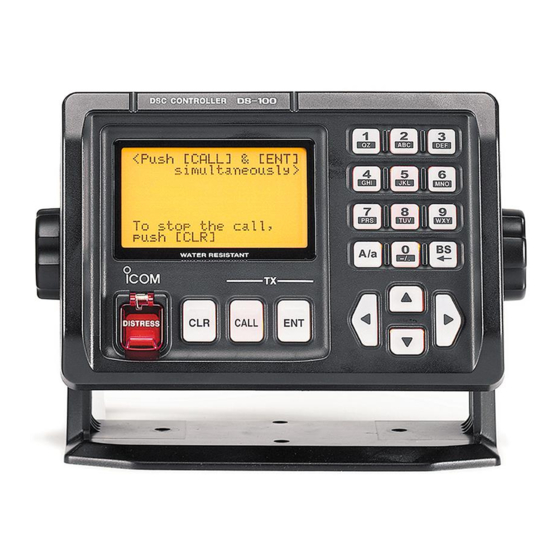
Summary of Contents for Icom DS-100
- Page 1 SERVICE MANUAL CLASS D/DSC TERMINAL DS-100...
- Page 2 This service manual describes the latest service information NEVER connect the terminal unit to an AC outlet or to a DC for the DS-100 CLASS D/DSC TERMINAL at the time of power supply that uses more than 16 V. This will ruin the terminal unit.
-
Page 3: Table Of Contents
TABLE OF CONTENTS SECTION 1 SPECIFICATIONS SECTION 2 INSIDE VIEWS SECTION 3 CIRCUIT DESCRIPTION 3 - 1 RECEIVER CIRCUITS ............. 3 - 1 3 - 2 PLL CIRCUIT . - Page 4 SECTION 1 SPECIFICATIONS ‘ ‘ GENERAL • Frequency coverage : 156.525 MHz (Ch 70) Rx only • Mode : 16K0G2B • Power supply requirement : 13.8 V DC (negative ground) • Usable temperature range : –20˚C to +60˚C • Current drain (at 13.8 V DC) : 1.0 A (approx.) : 50 Ω...
- Page 5 SECTION 2 INSIDE VIEWS • MAIN UNIT Speaker (SP1: PS1740P02) 2nd IF filter (FI3: ALFY450E) FM IF IC (IC1: TA31136FN) 1st mixer (Q2: 3SK166) Crystal filter (FI1, FI2: FL-310) DSC decoder VCO circuit (IC4: NJM2211M) Reference Oscillator PLL IC (IC2: µPD3140GS) (X2: CR-659 21.25 MHz) •...
-
Page 6: Circuit Description
SECTION 3 CIRCUIT DESCRIPTION 3-1 RECEIVER CIRCUITS The 1st IF signal from the IF amplifier is applied to the 2nd mixer section of the FM IF IC (IC1, pin 16), and is mixed with 3-1-1 RF AMPLIFER CIRCUIT (MAIN UNIT) the 2nd LO signal to be converted into a 450 kHz 2nd IF sig- The RF circuit amplifies signals within the range of frequen- nal. -
Page 7: Pll Circuit
3-2 PLL CIRCUIT 3-4 NMEA AND DATA INTERFACE 3-2-1 PLL CIRCUIT (MAIN UNIT) CIRCUITS A PLL circuit provides stable oscillation of the receiver 1st 3-4-1 NMEA CIRCUIT (MAIN UNIT) LO frequency. The PLL output compares the phase of the The NMEA signals (GGA) from OPC-945 are applied to IC5 divided VCO frequency to the reference frequency. -
Page 8: Logic Circuit
3-6 LOGIC CIRCUITS (LOGIC UNIT) • CPU Port IC1 is 16 bit single chip microcomputer and contains serial Description number name I/O, timer, A/D converter, D/A converter, programmable I/O, ROM and RAM. Outputs control signal for the LCD CADJ contrast. •... -
Page 9: Adjustment Procedures
: 100 kΩ ‘ ‘ CONNECTIONS Standard signal to the antenna connector generator –17 to –125 dBm (32 mV to 0.13 µV) DC power supply 13.8 V /15 A – + to DC cable Black DS-100 iM501EURO 4 - 1... -
Page 10: Reference And Receiver Adjustments
4-2 REFERENCE AND RECEIVER ADJUSTMENTS ADJUSTMENT MEASUREMENT POINT ADJUSTMENT ADJUSTMENT CONDITION VALUE UNIT LOCATION UNIT ADJUST LOCK • Receiving MAIN Connect a digital 2.1 V MAIN multi-meter or oscil- VOLTAGE loscope to check point CP3. REFERENCE • Receiving MAIN Connect a frequen- 134.825000 MHz MAIN FREQUENCY... - Page 11 • MAIN unit Reference frequency adjustment Lock voltage Lock voltage adjustment check point Reference frequency check point Sensitivity check point Sensitivity adjustment Squelch check point Squelch External SP adjustment connector 4 - 3...
-
Page 12: Parts List
SECTION 5 PARTS LIST [LOGIC UNIT] [LOGIC UNIT] ORDER ORDER DESCRIPTION DESCRIPTION ERJ3GEYJ 221 V (220 Ω) 1140008940 S.IC MB90F583BPFV-G 7030003360 S.RESISTOR ERJ3GEYJ 221 V (220 Ω) 1130009680 S.IC HN58X2432TI 7030003360 S.RESISTOR ERJ3GEYJ 221 V (220 Ω) 1130007450 S.IC RTC-4553A 7030003360 S.RESISTOR ERJ3GEYJ 221 V (220 Ω) 1110004710 S.IC... -
Page 13: Main Unit
[LOGIC UNIT] [MAIN UNIT] ORDER ORDER DESCRIPTION DESCRIPTION 4030007010 S.CERAMIC C1608 CH 1H 100D-T-A 1110003200 S.IC TA31136FN (EL) 4030006860 S.CERAMIC C1608 JB 1H 102K-T-A 1130007610 S.IC µPD3140GS-E1 (DS8) 4030006860 S.CERAMIC C1608 JB 1H 102K-T-A 1110003750 S.IC M5218AFP 600C 4030006860 S.CERAMIC C1608 JB 1H 102K-T-A 1110003650 S.IC NJM2211M-TE1... - Page 14 [MAIN UNIT] [MAIN UNIT] ORDER ORDER DESCRIPTION DESCRIPTION ERJ3GEYJ 100 V (10 Ω) 7030003200 S.RESISTOR R101 7030003490 S.RESISTOR ERJ3GEYJ 272 V (2.7 kΩ) ERJ3GEYJ 331 V (330 Ω) 7030003480 S.RESISTOR ERJ3GEYJ 222 V (2.2 kΩ) R102 7030003380 S.RESISTOR 7030003450 S.RESISTOR ERJ3GEYJ 122 V (1.2 kΩ) R103 7030003620 S.RESISTOR...
- Page 15 [MAIN UNIT] [MAIN UNIT] ORDER ORDER DESCRIPTION DESCRIPTION 4030006900 S.CERAMIC C1608 JB 1E 103K-T-A C152 4030006860 S.CERAMIC C1608 JB 1H 102K-T-A 4550006170 S.TANTALUM ECST1AY225R C153 4030006860 S.CERAMIC C1608 JB 1H 102K-T-A 4030006860 S.CERAMIC C1608 JB 1H 102K-T-A C154 4550006830 S.TANTALUM ECST1DY475R 4030011600 S.CERAMIC C1608 JB 1C 104KT-N...
- Page 16 8810008660 Screw PH BT M3 × 8 NI-ZU MP19 8810008660 Screw M3 × 8 SUS MP20 8810004540 MP21 8810006050 Icom screw E7 MP22 8930052290 O ring (AD) MP23 8850000690 Flat washer M3 (3×7×0.5) SUS Screw M3 × 8 SUS MP25...
- Page 17 MP21 (CH) MP23 (CH) MP22 (CH) MP7 (CH) MP25 (CH) J1 (CH) MP26 (CH) MP3 (CH) W1 (CH) MP20 (CH) MP1 (M) MP5 (CH) MP6 (CH) SP1 (M) W2 (CH) J3 (L) + BT1 (L) MAIN UNIT MP16 (CH) EP1 (CH) MP18 (CH) MP19 (CH) W2 (CH)
- Page 18 SECTION 7 SEMI-CONDUCTOR INFORMATION • TRANSISTORS AND FET’S • DIODES 2SA1362 GR 2SB1132 T100 R 2SC2714 Y 2SC4116 BL 2SC4215 O 1SS184 1SS355 DA204 U T107 HSU88TRF MA363 B (Symbol: AEG) (Symbol: BAR) (Symbol: QY) (Symbol: LL) (Symbol: QO) (Symbol: B3) (Symbol: A) (Symbol: K) (Symbol: 9)
-
Page 19: Logic Unit
SECTION 8 BOARD LAYOUTS 8-1 LOGIC UNIT • TOP VIEW 8 - 1... - Page 20 • BOTTOM VIEW to MAIN unit J3 8 - 2...
-
Page 21: Main Unit
8-2 MAIN UNIT • TOP VIEW DSC– DSC+ DATAM+ DATAM– DATAS+ DATAS– ICF3 to OPC-951 NMEAI+ NMEAI– NMEAO+ to OPC-945 ICF3 to LOGIC unit J1 8 - 3... - Page 22 SECTION 9 BLOCK DIAGRAM Q18, Q19 CH70 2SC4116 FI1, FI2 3stage 1stage 2SC2714 NJM2211M M5218AFP TA31136FN FL-310 3SK292 3SK166 DECODER FM IF IC X2 CR-659 (21.25MHz) IC10 TA7805F µPD3140GS 2SC4215 Q5 2SK210 Q15 2SB1132 D4, D5 MA363B Q16 DTC144TU 2SC4215 2SC4215 TA7808S RCEV...
- Page 23 SECTION 10 VOLTAGE DIAGRAM 10-1 LOGIC UNIT DS2-DS42 LCD BACKLIGHT SML-311YT KEY-1 KEY-4 KEY-7 DS14 DS15 DS16 DS27 KEY-A KEY-2 KEY-5 KEY-8 IC10B KEY-0 NJM2058M 330k 0.001 KEY-3 DS5 DS6 820k DS17 DS18 DS19 DS28 IC10A KEY-6 NJM2058M KEY-9 KEY-BS DS31 DS34 COM23...
- Page 24 10-2 MAIN UNIT DEMOD C143 0.01 0.022 0.001 0.001 0.001 0.001 0.01 CDBCA450CX24 R119 2.2µ 0.001 0.022 0.01 100k 0.001 0.001 0.001 0.01 0.01 0.001 GND1 20 VCC1 100p 100k 1.2k LS-440 PSTB VCC2 XB 17 0.001 470p 2.2k 0.82µ PDATA DATA 1.3k...
- Page 25 Fax : ( 604 ) 952-0090 Icom (UK) Ltd. : http://www.icomcanada.com Unit 9, Sea St., Herne Bay, Kent, CT6 8LD, U.K. Icom (Australia) Pty. Ltd. Phone : 01227 741741 Fax : 01227 741742 A.B.N. 88 006 092 575 : http://www.icomuk.co.uk 290-294 Albert Street, Brunswick, Victoria, 3056, Australia Icom France S.a...
- Page 26 S-13702HZ-CD-q C 2000 Icom Inc. 1-1-32, Kamiminami, Hirano-ku Osaka 547-0003, Japan...
Need help?
Do you have a question about the DS-100 and is the answer not in the manual?
Questions and answers