Table of Contents
Advertisement
Quick Links
VFD Driver/Controller IC
DESCRIPTION
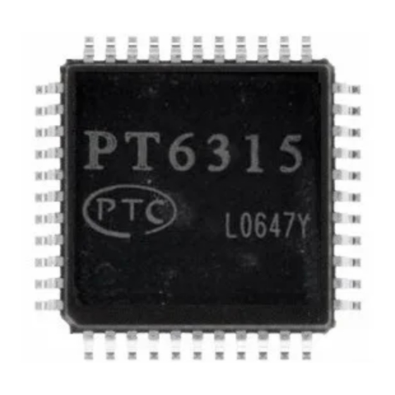
PT6315 is a Vacuum Fluorescent Display (VFD) Controller driven on a 1/4 to 1/12 duty factor. Sixteen
segment output lines, 4 grid output lines, 8 segment/grid output drive lines, one display memory, control circuit,
key scan circuit are all incorporated into a single chip to build a highly reliable peripheral device for a single chip
micro computer. Serial data is fed to PT6315 via a three-line serial interface. It is housed in a 44-pin, SSOP
and LQFP Package.
FEATURES
• CMOS Technology
• Low Power Consumption
• Key Scanning (16 x 2 matrix)
• Multiple Display Modes: (16 segments, 12 digits to 24 segments, 4 digits)
• 8-Step Dimming Circuitry
• LED Ports Provided (4 channels, 20 mA max.)
• Serial Interface for Clock, Data Input, Data Output, Strobe Pins
• No External Resistors Needed for Driver Outputs
• Available in 44-pin, SSOP and LQFP Package
APPLICATION
• Microcomputer Peripheral Device
PT6315 v2.0
Page 1
Tel : 886-2-29162151
Fax: 886-2-29174598
PT6315
Sep. 2002
Advertisement
Table of Contents

Related Manuals for PTC PT6315


Summary of Contents for PTC PT6315
- Page 1 Serial data is fed to PT6315 via a three-line serial interface. It is housed in a 44-pin, SSOP and LQFP Package.
-
Page 2: Block Diagram
Fax: 886-2-29174598 VFD Driver/Controller IC PT6315 BLOCK DIAGRAM SG1/KS1 SG2/KS2 SG3/KS3 SG4/KS4 SG5/KS5 SG6/KS6 SG7/KS7 SG8/KS8 SG9/KS9 SG10/KS10 SG11/KS11 SG12/KS12 SG13/KS13 SG14/KS14 SG15/KS15 SG16/KS16 SG21/GR8 SG22/GR7 SG23/GR6 SG24/GR5 Figure 1: PT6315 Internal Block Diagram PT6315 v2.0 Page 2 Sep. 2002... - Page 3 Tel : 886-2-29162151 Fax: 886-2-29174598 VFD Driver/Controller IC PT6315 PIN CONFIGURATION 44PIN LQFP LED1 SG19/GR10 LED2 SG18/GR11 LED3 SG17/GR12 LED4 SG16/KS16 DOUT SG15/KS15 SG14/KS14 SG13/KS13 SG12/KS12 SG11/KS11 SG10/KS10 Figure 2: PT6315 LQFP Pin Configuration PT6315 v2.0 Page 3 Sep. 2002...
- Page 4 SG23/GR6 SG22/GR7 SG21/GR8 SG20/GR9 SG19/GR10 LED1 SG18/GR11 SG17/GR12 LED2 LED3 LED4 SG16/KS16 SG15/KS15 DOUT SG14/KS14 SG13/KS13 SG12/KS12 SG11/KS11 SG10/KS10 SG9/KS9 SG8/KS8 SG7/KS7 SG6/KS6 SG1/KS1 SG5/KS5 SG2/KS2 SG3/KS3 SG4/KS4 Figure 3: PT6315 SSOP Pin Configuration PT6315 v2.0 Page 4 Sep. 2002...
-
Page 5: Pin Description
14 to SG1/KS1 to SG16/KS16 Also acts as the Key Source V E E Pull-Down Level 31 to SG17/GR12 to SG24/GR5 High Voltage Segment/Grid Output Pins 39 to GR4 to GR1 High-Voltage Grid Output Pins PT6315 v2.0 Page 5 Sep. 2002... -
Page 6: Functional Description
Commands determine the display mode and status of PT6315. A command is the first byte (b0 to b7) inputted to PT6315 via the DIN Pin after STB Pin has changed from “HIGH” to “LOW” State. If for some reason the STB Pin is set to “HIGH” while data or commands are being transmitted, the serial communication is initialized, and the data/commands being transmitted are considered invalid. - Page 7 PT6315 Display Mode and RAM Address Data transmitted from an external device to PT6315 via the serial interface are stored in the Display RAM and are assigned addresses. The RAM Addresses of PT6315 are given below in 8 bits unit.
- Page 8 COMMAND 2: DATA SETTING COMMANDS The Data Setting Commands executes the Data Write or Data Read Modes for PT6315. The data Setting Command, the bits 5 and 6 (b4, b5) are ignored, bit 7 (b6) is given the value of “1” while bit 8 (b7) is given the value of “0”.
- Page 9 PT6315 PT6315 Key Matrix & Key Input Data Storage RAM PT6315 Key Matrix consists of 16 x 2 array as shown below: Figure 6: PT6315 Key Matrix Each data inputted by each key are stored as follows. They are read by a READ Command, starting from the last significant bit.
- Page 10 PT6315 LED Display PT6315 provides 4 LED Display Terminals, namely LED1 to LED4. Data is written to the LED Port starting from the least significant bit (b0) of the port using a WRITE Command. Each bit starting from the least significant (b0) activates a specific LED Display Terminal -- b0 corresponds LED1 Display, b1 activates LED2 and so forth.
- Page 11 When power is turned ON, the address is set at “00H”. Please refer to the diagram below. Address: 00H to 23H Figure 10: Address Settings PT6315 v2.0 Page 11 Sep. 2002...
- Page 12 Please refer to the diagram below. When the power is turned ON, a 1/16 pulse width is selected and the displayed is turned OFF (the key scanning is stopped). Figure 11: Display Control Settings PT6315 v2.0 Page 12 Sep. 2002...
- Page 13 Internal Operating Frequency (fosc) = 224/T =500us Key Scan Data DISPLAY 9 10 1 Frame=T x (n +1) DISPLAY Figure 12: PT6315 Scanning & Display Timing Diagram Note: T is the width of Segment only PT6315 v2.0 Page 13 Sep. 2002...
- Page 14 PT6315 SERIAL COMMUNICATION FORMAT The following diagram shows the PT6315 serial communication format. The DOUT Pin is an N-channel, open- drain output pin, therefore, it is highly recommended that an external pull-up resistor (1 KOhms to 10 KOhms) must be connected to DOUT.
- Page 15 Tel : 886-2-29162151 Fax: 886-2-29174598 VFD Driver/Controller IC PT6315 SWITCHING CHARACTERISTIC WAVEFORM PT6315 Switching Characteristics Waveform is given below. where: PW (Clock Pulse Width)>400ns (Strobe Pulse Width)>1 t setup (Data Setup Time) >100ns (Data Hold Time)>100ns hold (Clock - Strobe Time)>1us (Fall Time)<150us...
- Page 16 Data 1 to n : Transfer Display Data (36 Bytes max.) Command 4: Display Control Command Figure 15: Display Memory Updated by Address Increments The following diagram shows the waveforms when updating specific addresses. Data Setting Command Address Setting Command Figure 16: Address Update PT6315 v2.0 Page 16 Sep. 2002...
- Page 17 5. When IC power is applied for the first time, the contents of the Display RAM are not defined; thus, it is strongly suggested that the contents of the Display RAM must be cleared during the initial setting. Figure 17: Recommended Software Flowchart PT6315 v2.0 Page 17 Sep. 2002...
-
Page 18: Absolute Maximum Ratings
- 1 5 ( S e g m e n t ) RECOMMENDED OPERATING RANGE (Unless otherwise stated, Ta=-20 to +70 C, GND=0V) Parameter Symbol Min. Typ. Max. Unit Logic Supply Voltage High-Level Input Voltage 0.7V Low-Level Input Voltage 0.3V Driver Supply Voltage PT6315 v2.0 Page 18 Sep. 2002... -
Page 19: Electrical Characteristics
C o n s u m p t i o n D D d y n D i s p l a y O F F Note: The frequency value is for PTC test condition. fosc=224/T If you want to know details data, please see page 13. PT6315 v2.0 Page 19 Sep. - Page 20 C o n s u m p t i o n D D d y n D i s p l a y O F F Note: The frequency value is for PTC test condition. fosc=224/T If you want to know details data, please see page 13. PT6315 v2.0 Page 20 Sep.
- Page 21 12 13 14 1 5 16 1 7 18 19 20 21 22 0.1 F 1N4148 x 16 Figure 18: PT6315 LQFP Applicaiton Circuit Note: The capacitor (0.1uF) connected between the GND and the VDD pins must be located as close as possible to the PT6315 chip.
- Page 22 100K PT6315 0.1 F 1N4148 X 16 Figure 19: PT6315 SSOP Applicaiton Circuit Note: The capacitor (0.1uF) connected between the GND and the VDD pins must be located as close as possible to the PT6315 chip. PT6315 v2.0 Page 22...
-
Page 23: Order Information
P T 6 3 1 5 PT6315-S 44 pin SOP Package PT6315-S PT6315 L or "L"in circle 44 pin LQFP Package P T 6 3 1 5 PT6315-S L or "L"in circle 44 pin SOP Package PT6315-S Note: 1. L = Lead Free 2. The Lead Free mark is put in front of the date code. PT6315 v2.0 Page 23 Sep. 2002... -
Page 24: Package Dimension
Tel : 886-2-29162151 Fax: 886-2-29174598 VFD Driver/Controller IC PT6315 PACKAGE DIMENSION 44-Pin LQFP Package (Body Size: 10mm x 10mm; Pitch: 0.80mm; THK Body: 1.40mm) SEATING PLANE GAUGE PLANE 0.25mm PT6315 v2.0 Page 24 Sep. 2002... - Page 25 8. A1 is defined as the distance from the seating plane to the lowest point on the package body. 9. Refer to JEDEC STD MS-026 Variation BCB JEDEC is the trademark of JEDEC SOLID STATE TECHNOLOGY ASSOCIATION PT6315 v2.0 Page 25 Sep. 2002...
- Page 26 45 0.004 SEATING PLANE Notes: 1. Dimension D do not include mold flash, protrusions or gate burrs. 2. Mold flash, protrusions or gate burrs shall not exceed 0.006 inch (0.152 mm) per side PT6315 v2.0 Page 26 Sep. 2002...
Need help?
Do you have a question about the PT6315 and is the answer not in the manual?
Questions and answers