Table of Contents
Advertisement
Quick Links
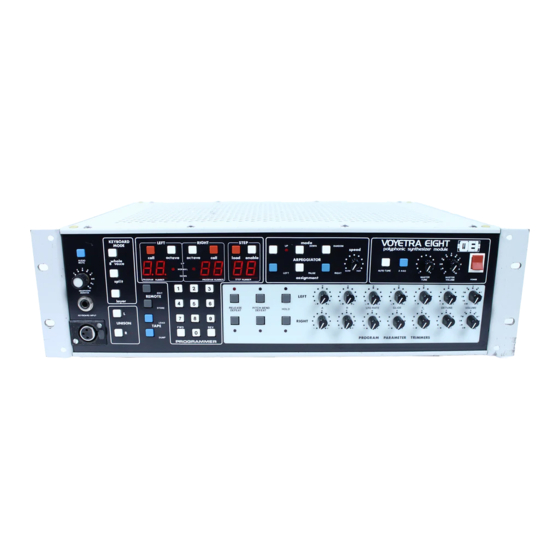
Voyetra Eight Hardware Maintenance Manual
Revision
Date
1.0
??/??/1984 Carmine J. Bonanno
1.0a
06/19/2002 Joan Touzet
"Copywright [sic] 1984 by OCTAVE-PLATEAU ELECTRONICS, INC.
Revision 1.0a
Changed By
joant@ieee.org
http://www.atypical.net/
51 Main Street
Yonkers, New York 10701"
Reason
Original Revision
Mistake correction
Revisions for clarity
Started schematic entry
Advertisement
Table of Contents
Troubleshooting

Related Manuals for Octave Voyetra Eight


Summary of Contents for Octave Voyetra Eight
- Page 1 Revision 1.0a Revision Date Changed By Reason ??/??/1984 Carmine J. Bonanno Original Revision 1.0a 06/19/2002 Joan Touzet Mistake correction joant@ieee.org Revisions for clarity http://www.atypical.net/ Started schematic entry “Copywright [sic] 1984 by OCTAVE-PLATEAU ELECTRONICS, INC. 51 Main Street Yonkers, New York 10701”...
-
Page 2: Table Of Contents
Letter “A” appears ....................... 15 3.7.2 Letter “B,” “C” or “D” appears ..................16 3.7.3 Letter “E” appears or other pulse width problems .............. 16 3.7.4 No sub octave........................16 VCF CARD ............................17 ......................17 HEORY OF PERATION VCF O ........................ - Page 3 ........................19 IGNALS 4.6.1 Inputs ............................ 19 4.6.2 Outputs..........................20 VCF C ..................20 ROUBLESHOOTING 4.7.1 Step 00-02: Resonance (Q) Tests ..................20 4.7.2 Step 03: DC Feedthrough Check ..................20 4.7.3 Step 04-11: Initial F and V/Oct Calibration ............... 20 4.7.4 Step 11-27: VCO Volume Test .....................
-
Page 4: Introduction
Introduction Tracking Down Voices From time to time, this manual will refer to calibrations for a particular voice. These voices are numbered from 0-7 and are indicated on the trimmer locations diagram. However, when troubleshooting, it is often necessary to determine which voice is defective. The Set Page (see appendix) provides a feature for disabling voices which may be used to locate which voice is sounding. - Page 5 First, determine what it is about the voice that is “different.” Is it the “tone?” Then it may need a VCF calibration. Is it the “level?” Then it may be a VCA calibration. Is it the “tuning?” Then it may need a Mod System calibration, or a VCO may be defective.
-
Page 6: Card Summary
Card Summary 1.4.1 Mixer Card Contains eight VCAs (one per voice) and a stereo mixer that sums the system outputs. Calibrations include CVA offset trimmers and channel gain trimmers. The MIXER also contains the Noise Source and various other minor system functions. 1.4.2 VCO Card Contains four VCOs. -
Page 7: Pot Panel
1.4.9 Pot Panel Contains the Keyboard and front panel parameter trimmer interface circuits. Calibrations include pitch bend balance and gain, and X axis gains. 1.4.10 Switch Panel Contains LEDs and switches with interfacing circuits for connecting them to the CPU. 1.4.11 Jack Bay Contains interface jacks and an AGC circuit for the Tape input. -
Page 8: Signal Flow Diagrams
Signal Flow Diagrams The following diagrams are included to assist in understanding some of the Voyetra 8’s signal flow paths. Mod Bank VCO1, VCO2 F VCAs VCO1 VCO1 VCO2 VCO2 Mono Contr. DIGI ANA1 ANA2 CPU +/-x, Press (Mono Controllers) Figure 1-2 Modulation System Signal Flow JACK DIGI... -
Page 10: Mixer Card
MIXER Card Theory of Operation The MIXER Card consists of eight identical Voltage Controlled Amplifier (VCA) circuits followed by mixing circuitry. In addition, certain other related functions are placed on this card. The functions on this board include: • Eight channel demultiplexer for ADSR 2 voices 0-7 •... -
Page 11: Headphones
them on the MIXER CARD at the points called VOLUME L, R. The Master Volume Pot is routed to the JACK BAY for processing by the external Volume Pedal, and then routed to the MIXER CARD to the point labeled MASTER VOL. These control signals are multiplied by VCAs that convert them to control currents used to derive the volume/noise gate VCAs as illustrated on the schematic. -
Page 12: Vco Card
100% width value. This causes the pulse width to go high, which is inverted by a transistor that feeds the mixer. The sub- octave is turned off by the DAC when it toggles the rest line on the CD4520 divider. -
Page 13: Autotune Functionality
AutoTune functionality When the front panel AUTOTUNE button is pressed, the CPU CARD calibrates the VCO tracking (V/Octave), initial pulse width, and initial frequency. The CPU first turns off all of the VCO waveforms except for the Sawtooth and disables the VCO pitchbend lines coming from ANAMOD 2. -
Page 14: Dc Voltages
Each letter corresponds to a different problem, but the only serious one is “A” since it indicates that the VCO can’t be sensed by the CPU, either because it is very low in frequency, has a DC offset on it, or is completely missing. -
Page 15: Step 50-71: Waveform Tests
suggestions will still prove useful if the theory section has been thoroughly understood. 3.6.1 Step 50-71: Waveform Tests These steps check that all of the VCO waveforms are present and are of proper amplitude and frequency. Since the instrument has been AUTOTUNEd and the middle A key is down, the outputs should all be pretty close to A440. -
Page 16: Letter "B," "C" Or "D" Appears
The voltage at the CEM3340 pin 5 should be about +6V or the Pulse wave won’t turn off. 3.7.4 No sub octave Check if the input to the CD4520 has a negative spike on it. If it doesn’t, then check the coupling cap and bias resistors on the input to the CD4520. -
Page 17: Vcf Card
Theory of Operation The Voltage Controlled Filter Card (VCF Card) consists of four identical four-pole (-24dB/Octave) VCF circuits based on the SSM 2044 Integrated Filter. One card is used for the LEFT side of the instrument and the other for the RIGHT side of the instrument. Both cards are identical and may be interchanged to facilitate troubleshooting. -
Page 18: Calibrations
“V/Oct” is set so that a change of one volt at the summer input produces a one octave change in filter frequency. The control voltage is scaled down to less than +/- 100mV at the SSM2044 input pin 13 to obtain the full sweep range of 20 Hz –... -
Page 19: Vco Multiplexing System
key is pressed on the keyboard (assuming that the test programs have been loaded.) The “Q CAL” trimmer is used to set all VCFs so that they oscillate at the same resonance setting. When set properly, all of the VCFs should burst into oscillation at the same point on the front panel Q control pot. -
Page 20: Outputs
• CPU control signals for the CD4051 demultiplexers (EN 15, EN 9, AL0, AL1, AL2) coming from DIGIMOD • Modulation scan clocks (MODEN, MA0, MA1) • VCO multiplexer clocks (VMA0, VMA1) • DAC control line (Bypass) • VCO1 & VCO2 audio inputs for four voices from VCO cards •... -
Page 21: Step 11-27: Vco Volume Test
ADSR modulation depth. Problems can first be traced to the LM324 U6, but proper functioning of this IC is assured if the output follows the input. The input levels on the resistor network associated with this summing amp should be checked for conformity with a good amp. Problems with the ADSR can be traced to the output buffers/demux circuit formed by U17 (TL064) and U4 (CD4051). - Page 22 determined by their offset voltage) they can cause the VCOs to jitter and sound unstable. In this step, the outputs of the TL068s are examined at a high scope sensitivity to weed out potentially bad ones. The inputs to the CD4052s are all 0V, so the TL068 outputs should be 0V as well (within +/- 5mV.)
-
Page 23: Digimod Card
DIGIMOD Card Theory of Operation The DIGIMOD Card contains miscellaneous digital and analog circuitry for modulation system and CPU card support. The functions on this board include: • Demultiplexing enable signals for system CD4051s • Velocity and ADSR 2 demultiplexing/remultiplexing for the modulation system •... -
Page 24: Modulation System Scan Clocks
To select the specific CD4051 to be enabled, the CPU addresses one of the 16 locations on CD4515 U15, which is a 4-to-16 decoder whose outputs are normally high. When addresses, the output goes low, enabling one of the 16 CD4051s memory mapped into the system. The particular CD4051 connected to each output enable pin is labeled on U15. -
Page 25: Mono Controller Multiplexer
Mono Controller Multiplexer When mono controllers are selected in the MOD BANKS, the CPU loads the respective cell in the LS670 4x4 dual port RAMs. The outputs of these RAMs are constantly scanned by the mod system and switch the controllers on or off via the CD4016 analog switch U3. -
Page 26: Keyboard
Keyboard Theory Of Operation The keyboard receives power and clock information from the VOYETRA module. It uses this clock information to synchronize the acquisition of keyboard and analog controller signals which are multiplexed and sent to the VOYETRA module. The functions in the keyboard include: •... -
Page 27: Digital Data Acquisition
The attenuated CLOCK signal transitions occur between +9V to +5V, so the top comparator is biased at about +6V to detect it. This detected signal, called CK (clock), is used to gate the shift register CD4015 U5 and the CD4021 parallel-to-serial converters U12-U27. The attenuated DIGISTROBE signal is between +9V and +2.5V, thus the threshold for the next comparator is about +4V. -
Page 28: Analog Data Acquisition
three clock pulses. Thus, whenever the VOYETRA module wants to see the state of a key, it sends a clock pulse and the next cell is advanced. The output of the CD4021s is routed to the CD4051 U8 address pins, while the inputs to the CD4051 are three voltage levels: +8V, -6V and ground. -
Page 29: Joystick
6.2.6 Joystick The joystick is biased by +8V and the X & Y potentiometers are processed by identical opamp level shifters that are used to set zero volts out for vertical joystick position. The outputs of these circuits are followed by balance trimmers to adjust the gain in both directions. Calibrations Pressure calibrations include offset for left and right pressure sensors, gain adjustment for left and right pressure sensors, gain adjustment for... -
Page 30: Pot Panel
Pot Panel Theory of Operation The Pot Panel serves two major functions: Keyboard Interfacing. The VPK-5 keyboard clock/power signal is generated under control of the CPU. The keyboard digital data is detected and sent to the CPU. The keyboard analog data is demultiplexed and routed to the DIGIMOD card. -
Page 31: Keyboard Data Interface
• Analog Clock Off (ACKOFF): When the CPU is done receiving analog data, it turns off the analog clock by writing to 74LS138 position 7. Note that in normal operation, all of these outputs should be active so that a Logic Probe connected to any of these lines will flash to indicate the presence of pulses. -
Page 32: Analog Data Retrieval
and key down information is determined by the Chip Select (CS) lines CS UB (for Upper Bus, or Key Up) and CS LB (for Lower Bus, or Key Down). Again, since the CPU will always be accessing the keyboard, these lines should always be active. -
Page 33: Calibrations
Calibrations The calibrations on the pot panel are associated with the pitch bend and X controller. The pitch bend that is received from the keyboard must be adjusted so that the up and down range is consistent between VOYETRA modules. Thus, the trimmer/diode network that follows the pitch bend buffer allows balance to be set, while the gain controls for pitch bend left and right adjust for pitch bend range uniformity in both left and right halves of the instrument.
Need help?
Do you have a question about the Voyetra Eight and is the answer not in the manual?
Questions and answers