Table of Contents
Advertisement
Quick Links
VP3500 User Manual • Document Number 101-3500-0001 • Revision A0
Engineering, LLC
Model VP3500 User Manual
6U VPX Dual PMC, XMC, MiniPCIe Carrier card with Integrated 5-Port Gigabit Ethernet Switch
Property of Rigel Engineering, LLC.
Confidential & Proprietary
690 Cone Park Court
Merritt Island, Florida 32952
Revision A0
Information subject to change
October 9, 2013
Document Number 101-3500-0001
page 1
Property of Rigel Engineering, LLC. Confidential & Proprietary
690 Cone Park Court, Merritt Island, Florida 32952
Advertisement
Table of Contents

Summary of Contents for Rigel VP3500
- Page 1 VP3500 User Manual • Document Number 101-3500-0001 • Revision A0 Engineering, LLC Model VP3500 User Manual 6U VPX Dual PMC, XMC, MiniPCIe Carrier card with Integrated 5-Port Gigabit Ethernet Switch Property of Rigel Engineering, LLC. Confidential & Proprietary 690 Cone Park Court...
- Page 2 Copyright © 2013 Rigel Engineering, LLC. All rights reserved. No portion of this publication or product model VP3500 (hardware or software design) may be copied in any form or by any means (including but not limited to electronic, photocopying, or otherwise) without the prior written permission of Rigel Engineering, LLC.
-
Page 3: Table Of Contents
VP3500 User Manual • Document Number 101-3500-0001 • Revision A0 Contents Section 1 : Introduction 1.1 : Overview ............................9 1.2 : Feature list ........................... 10 1.3 : Related documents ........................10 1.4 : Features overview ........................12 1.4.1 : VPX Backplane Fabric ...........................12 1.4.2 : Two PMC Slots............................12... - Page 4 VP3500 User Manual • Document Number 101-3500-0001 • Revision A0 Section 3 : Interconnections and Pinouts 3.1 : VP3500 Connectors ........................27 3.2 : VPX Connectors .......................... 28 3.2.1 : VPX P0 ..............................28 3.2.2 : VPX P1 ..............................30 3.2.3 : VPX P2 ..............................32 3.2.4 : VPX P3 ..............................33...
- Page 5 VP3500 User Manual • Document Number 101-3500-0001 • Revision A0 5.2 : PCIe Switch ..........................83 5.3 : Microcontroller Interface ......................84 5.3.1 : Microcontroller Serial Port ........................84 5.3.2 : Microcontroller Serial Port Commands ....................85 5.3.2.1 : Select I2C Bus ..........................85 5.3.2.2 : Select I2C Slave Address ........................86...
- Page 6 VP3500 User Manual • Document Number 101-3500-0001 • Revision A0 Section 1 : List of Tables Table 1 : Table of Acronyms ........................8 Table 2 : VPX P0 Signals ........................28 Table 3 : VPX P1 Signals ........................30 Table 4 : VPX P2 Signals ........................
- Page 7 Table 43 : PCIe LEDs .......................... 82 Table 44 : PCIe LED Pattern ....................... 82 Table 45 : RT3500 Connector & VP3500 HDR3 Serial Pins ............... 84 Table 46 : Microcontroller Serial Port Commands ................85 Table 47 : Microcontroller VPX Commands ..................90 Table 48 : Power Status ........................
- Page 8 VP3500 User Manual • Document Number 101-3500-0001 • Revision A0 Section 2 : List of Figures Figure 1 : VP3500 ..........................9 Figure 2 : VP3500 - Block Diagram ......................11 Figure 3 : Picture of IO Module ......................15 Figure 4 : RT3500-0000 ........................17 Figure 5 : Ordering Information ......................
- Page 9 VP3500 User Manual • Document Number 101-3500-0001 • Revision A0 Acronym Description A term used to describe double high VME, VME64 , and VME64x boards that are 233.35 mm in height. Also used to describe backplanes that interface to these same boards.
-
Page 10: Section 1 : Introduction
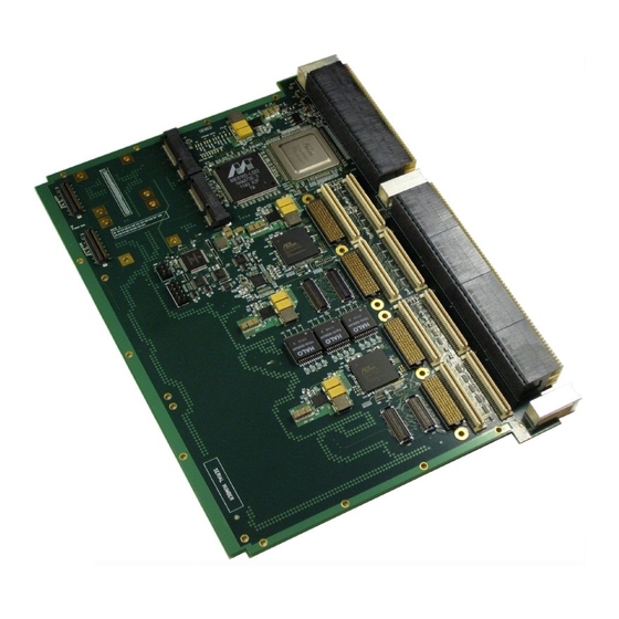
Figure 1 : VP3500 1.1 : Overview Rigel’s VP3500 6U VPX carrier card presents system designers with the ability to incorporate a wide variety of functionality to any 6U VPX system. The VP3500 features two PMC/XMC slots, two MiniPCIe sockets, and an integrated 5-port Gigabit Ethernet switch (VITA 46.6). The VP3500 is available in various ruggedization levels including commercial or extended temperature, air or conduction-cooled and rugged versions for harsh environments. -
Page 11: Feature List
• On-board temperature sensor 1.3 : Related documents The VP3500 incorporates several features that may not be covered in this manual and may require the user to reference external documentation for the required information. The following is a list of related documentation that may be helpful. - Page 12 VP3500 User Manual • Document Number 101-3500-0001 • Revision A0 Model VP3500 PCI-X 133MHz PCIe to PCI-X Bridge PCIe x8 PCIe x4 PCIe x4 Mini PCIe PCIe x4 PCIe PCIe x1 PCIe x4 Switch PCIe x4 2x 1000Base-BX P64s RIO...
-
Page 13: Features Overview
(see section 5.3). The PCIe switch interfaces the VPX backplane as four, 4-lane PCI Express links to P1 (VITA 46). Although the VP3500 switch defaults to a four, 4-lane interface, it also allows for port widths of x1, x2, x8, and x16 to support specific bandwidth and backplane requirements. -
Page 14: Two Minipcie Sockets
Another challenge is cooling the MiniPCIe cards. A standard air or conduction-cooled frame will not likely work since all MiniPCIe cards are different. The VP3500 heat frames are designed with a removable section for the MiniPCIe cards. This allows a specific heat-frame solution for each set of MiniPCIe cards. -
Page 15: Management Microcontroller
1.4.6 : Management Microcontroller The on-board management microcontroller allows continuous communication between the system controller and the VP3500. The microcontroller is used to reconfigure the VP3500 from its standard option settings, monitors the on-board power supplies and ambient board temperature. The microcontroller reports status and responds to system controller commands. -
Page 16: Io Modules
1.5.2 : IO Modules Rigel Engineering’s VP3500 may host any combination of PMC and XMC cards. Each PMC/XMC has a pluggable IO module that route either XMC or PMC single-ended IO signals to the VPX backplane per VITA specification 46.9. -
Page 17: Minipcie Rear Io Adapter
One of the challenges of using MiniPCIe cards is the lack of a standard for accessing the card’s IO signals. The VP3500 has addressed this by providing a custom adapter card that bridges the MiniPCIe’s IO signals to the VPX backplane. - Page 18 VP3500 User Manual • Document Number 101-3500-0001 • Revision A0 Serial Port HDR1 HDR2 Power Switch GbE P5 GbE P4 GbE P1 HDR3 GbE P0 GbE P2 Reset Switch RT3500-0000 Figure 4 : RT3500-0000 page 18 Property of Rigel Engineering, LLC. Confidential & Proprietary...
-
Page 19: Ordering Information
VP3500 User Manual • Document Number 101-3500-0001 • Revision A0 1.6 : Ordering Information The VP3500 may be ordered by the specific model numbers as outlined in the below Figure. The VP3500 may also be ordered with customer-specific options. Please contact Rigel support for further details. -
Page 20: Section 2 : Configuration And Installation
The VP3500 PMC slots support +3.3v signaling or universal PMC cards. The VP3500 PCI IO signaling level is +3.3v. Damage may occur to the VP3500 if a PMC module drives +5v signal levels. Proper PMC signal voltage keying is provided on the VP3500. - Page 21 VP3500 User Manual • Document Number 101-3500-0001 • Revision A0 Microcontroller Serial Header MiniPCIe 1 Rear IO Adapter Connector MiniPCIe 1 MiniPCIe 2 Rear IO Adapter Connector MiniPCIe 2 PMC/XMC 1 PMC/XMC 2 Figure 6 : VP3500 Feature Identification page 21 Property of Rigel Engineering, LLC.
-
Page 22: Air-Cooled Pmc Installation And Removal
1. Attach an ESD wrist strap to your wrist and securely attach the other end to chassis ground. 2. Turn the system power off and disconnect the AC plug from the system. 3. Carefully remove the VP3500 from the VPX chassis and place it on a cushioned, flat surface. An ESD pad is the ideal option. -
Page 23: Conduction-Cooled Pmc Installation And Removal
1. Attach an ESD wrist strap to your wrist and securely attach the other end to chassis ground. 2. Turn the system power off and disconnect the AC plug from the system. 3. Carefully remove the VP3500 from the VPX chassis and place it on a cushioned, flat surface. An ESD pad is the ideal option. -
Page 24: Air-Cooled Xmc Installation And Removal
1. Attach an ESD wrist strap to your wrist and securely attach the other end to chassis ground. 2. Turn the system power off and disconnect the AC plug from the system. 3. Carefully remove the VP3500 from the VPX chassis and place it on a cushioned, flat surface. An ESD pad is the ideal option. -
Page 25: Conduction-Cooled Xmc Installation And Removal
4. Carefully align and slide the MiniPCIe card into its socket. 5. Install the MiniPCIe mounting screws to the heat frame on the top side of the VP3500. Tighten the screws. Rugged applications should use Loctite 242 (or similar) on the threads. -
Page 26: Minipcie Rear Io Module Installation And Removal
5. Carefully align the IO module’s connectors to the connectors on the VP3500 and press down firmly. 6. Install the IO module’s mounting screws to the heat frame on the top side of the VP3500. Tighten the screws. Rugged applications should use Loctite 242 (or similar) on the threads. -
Page 27: Required Equipment
3. Follow previous steps to install PMC/XMCs and MiniPCIe cards. 4. Carefully slide the VP3500 into a VPX payload slot. Take caution to seat the card firmly in the chassis by using the ejector handles. If you are using a conduction-cooled model, tighten the wedge locks. -
Page 28: Section 3 : Interconnections And Pinouts
VP3500 User Manual • Document Number 101-3500-0001 • Revision A0 Section 3 : Interconnections and Pinouts 3.1 : VP3500 Connectors This section provides signal information for the connectors on the VP3500. MP1 IO MP2 IO Figure 7 : VP3500 Connectors page 28 Property of Rigel Engineering, LLC. -
Page 29: Vpx Connectors
These low-true input pins are defined for system-wide geographical addressing. They are pulled up on the VP3500 to +3.3V and are routed to the microcontroller. The microcontroller uses these signals to determine the slot the card is plugged into and defines it IPMI (I2C) addressing. - Page 30 This also supports the updating or protection of program store memory. This high-true input signal to the VP3500 is routed to the NVMRO pins on each XMC connector and the on-board EEPROM write protect pin.
-
Page 31: Vpx P1
Open VPX Standard (VITA 65) defines the data plane as a plane that is used for application and external data traffic. The VP3500 implements all 16 PCIe lanes as the data path to communicate with other boards in the system. - Page 32 37. Default as an input. These signals are the 16 differential PCIe lanes that make up the VP3500’s VPX data plane. The default configuration for the data plane is a 4x4 but may be configured as 1x16 or 2x8 as well. The ports will also auto negotiate to fewer lanes if the full port width is not supported.
-
Page 33: Vpx P2
The VP3500 uses this plane to route the majority of its MiniPCIe custom IO connector to the VPX backplane. Each of the two MiniPCIe custom IO connectors have 20 differential and 8 single-ended signals where the first 16 differential and 4 single-ended are routed to P2 as illustrated below. -
Page 34: Vpx P3
VPX P3 is defined per VITA Standard 46.9 which maps PMC 1 (P14) and XMC 1 (J16) single-ended user IO pins to VPX P3. The VP3500 supports either P64s or X38s by selecting a pluggable IO module mounted on the card. For XMC IO use model number IM3500-0000 and for PMC use IM3500-0001. For information on IO module pin mapping please refer to sections 3.3.3 &... - Page 35 RS232_RX RS-232 level Receive data pin to the microcontroller serial data in pin 34. PLT_RST_L VP3500 Platform reset output signal. This is an open collector type output to a rear transition module (RTM). UC_BKGD The Microcontroller background signal to the programming/debug header on the RTM.
-
Page 36: Vpx P4
VITA 46.6 Gigabit Ethernet Control Plane on VPX P4 routing. PWRDWN_L VP3500 Power down/up toggle. A LVTTL low-true input signal (pulled up on the VP3500) to power control circuitry. A momentary switch to ground or pulling this signal low will toggle the VP3500 power on/ off circuitry. RST_IN_L Reset in. -
Page 37: Vpx P5
VPX P5 is defined per VITA Standard 46.9 which maps PMC 2 (P24) and XMC 2 (J26) single-ended user IO pins to VPX P5. The VP3500 supports either P64s or X38s by selecting a pluggable IO module mounted on the card. For XMC IO use model number IM3500-0000 and for PMC use IM3500-0001. For information on IO module pin mapping please refer to section 3.3.3 &... -
Page 38: Vpx P6
VP3500 User Manual • Document Number 101-3500-0001 • Revision A0 3.2.7 : VPX P6 VPX P6 is defined per VITA standard 46.9 which defines the signal mapping of XMC 2 (J26) differential user IO pins to VPX P6 (X12d+X8d). This connector also includes the upper 4 single-ended signals and differential pairs of each MiniPCIe custom connector plus the 5th Gigabit Ethernet port. -
Page 39: Xmc Connectors
3.3.1 : XMC 1 There are two connectors for XMC site 1 on the VP3500. J15 has the standard XMC PCIe signals (VITA 42.3) and J16 has the user defined IO signals which are dependent on what the XMC card supports. - Page 40 If this signal is used, it shall be asserted low at the de-assertion of RESET_L to indicate that the XMC is performing self-test and is not yet ready. This VP3500 input signal is pulled up to +3.3V through an 8.2K ohm resistor and routed to microcontroller pin 53.
- Page 41 The VP3500 provides +5V to its XMC VPWR pins. RESET_L XMC Reset In. When this signal is asserted low by the VP3500, the mezzanine card shall initialize itself into a known state. This signal is the platform reset for the VP3500.
- Page 42 VP3500 User Manual • Document Number 101-3500-0001 • Revision A0 Row A Row B Row C Row D Row E Row F XMC_1_A1 XMC_1_B1 XMC_1_C1 XMC_1_D1 XMC_1_E1 XMC_1_F1 XMC_1_C2 XMC_1_F2 XMC_1_A3 XMC_1_B3 XMC_1_C3 XMC_1_D3 XMC_1_E3 XMC_1_F3 XMC_1_C4 XMC_1_F4 XMC_1_A5 XMC_1_B5...
-
Page 43: Xmc 2
3.3.2 : XMC 2 There are two connectors for XMC site 2 on the VP3500. J25 has the standard XMC PCIe signals (VITA 42.3) and J26 has the user defined IO signals which are dependent on what the XMC card supports. - Page 44 If this signal is used, it shall be asserted low at the de-assertion of RESET_L to indicate that the XMC is performing self-test and is not yet ready. This VP3500 input signal is pulled up to +3.3V through an 8.2K ohm resistor and routed to microcontroller pin 54.
- Page 45 The VP3500 provides +5V to its XMC VPWR pins. RESET_L XMC Reset In. When this signal is asserted low by the VP3500, the mezzanine card shall initialize itself into a known state. This signal is the platform reset for the VP3500.
- Page 46 VP3500 User Manual • Document Number 101-3500-0001 • Revision A0 Row A Row B Row C Row D Row E Row F XMC_2_A1 XMC_2_B1 XMC_2_C1 XMC_2_D1 XMC_2_E1 XMC_2_F1 XMC_2_C2 XMC_2_F2 XMC_2_A3 XMC_2_B3 XMC_2_C3 XMC_2_D3 XMC_2_E3 XMC_2_F3 XMC_2_C4 XMC_2_F4 XMC_2_A5 XMC_2_B5...
-
Page 47: Io Module (Xmc)
The IO module has two 60-pin connectors. If a PMC is installed instead, the PMC IO module should be used. See section 3.4.3 for additional information regarding the PMC IO Module. The following tables describe the single-ended signal mapping for both XMC slots when using Rigel model number IM3500-0000 IO module. - Page 48 VP3500 User Manual • Document Number 101-3500-0001 • Revision A0 ‘ XMC_1 VITA 46.9 X38s single-end signals from XMC slot 1 J16. ‘ XMC_1 VITA 46.9 X38s single-end signals to VPX connector P3. PXMC_1_ID_1,0 These two pins are module identification pins. These signals may be read by the microcontroller. The XMC X38s module (IM3500-0000) ID pins are read as 00, respectively.
- Page 49 VP3500 User Manual • Document Number 101-3500-0001 • Revision A0 IO Module Pin Notes Signal Name Notes IO Module Pin XMC_1_F5 To VPX P3 A5 XMC_1_C6 To VPX P3 F6 XMC_1_F6 To VPX P3 C6 XMC_1_C7 To VPX P3 E6...
- Page 50 VP3500 User Manual • Document Number 101-3500-0001 • Revision A0 IO Module Pin Notes Signal Name Notes IO Module Pin XMC_2_F1 XMC_2_C1 XMC_2_F2 XMC_2_C2 XMC_2_F3 XMC_2_C3 XMC_2_F4 XMC_2_C4 XMC_2_F5 XMC_2_C5 XMC_2_F6 XMC_2_C6 XMC_2_F7 XMC_2_C7 XMC_2_F8 XMC_2_C8 XMC_2_F9 XMC_2_C9 XMC_2_F10 From XMC J26...
- Page 51 VP3500 User Manual • Document Number 101-3500-0001 • Revision A0 ‘ XMC_2 VITA 46.9 X38s single-end signals from XMC slot 2 J26. ‘ XMC_2 VITA 46.9 X38s single-end signals to VPX connector P5. PXMC_2_ID_1,0 These two pins are module identification pins. These signals may be read by the microcontroller. The XMC X38s module (IM3500-0000) ID pins are read as 00, respectively.
- Page 52 VP3500 User Manual • Document Number 101-3500-0001 • Revision A0 IO Module Pin Notes Signal Name Notes IO Module Pin XMC_2_F5 To VPX P5 A5 XMC_2_C6 To VPX P5 F6 XMC_2_F6 To VPX P5 C6 XMC_2_C7 To VPX P5 E6...
-
Page 53: Pmc Connectors
3.4.1 : PMC 1 There are four connectors for PMC site 1 on the VP3500, J11, J12, J13 and J14. J11, J12 and J13 make up the standard 64-bit PCI-X bus and J14 has user defined IO signals which depends on what the PMC card supports. - Page 54 VP3500 User Manual • Document Number 101-3500-0001 • Revision A0 Signal Name -12V_AUX INTA_L INTB_L INTC_L PMC_PRESENT_L INTD_L +3.3V_AUX GNT0_L REQ0_L +3.3V (VIO) AD31 AD28 AD27 AD25 CBE3 AD22 AD21 AD19 +3.3V (VIO) AD17 FRAME_L IRDY_L DEVSEL_L PCIXCAP LOCK_L SDONE_L SBO_L +3.3V (VIO)
- Page 55 ‘ Rose Standard PCI or PCI-X signals. BMODE 4, 3, 2 These input signals to the PMC are set to 001 by the VP3500, respectively. This should return PMC module present status from the PMC. page 55 Property of Rigel Engineering, LLC. Confidential & Proprietary...
- Page 56 VP3500 User Manual • Document Number 101-3500-0001 • Revision A0 Signal Name CBE7 CBE6 CBE5 CBE4 +3.3V PAR64 AD63 AD62 AD61 AD60 AD59 AD58 AD57 +3.3V AD56 AD55 AD54 AD53 AD52 AD51 AD50 AD49 AD48 AD47 AD46 AD45 +3.3V AD44...
- Page 57 VP3500 User Manual • Document Number 101-3500-0001 • Revision A0 Signal Name PMC_1_1 PMC_1_2 PMC_1_3 PMC_1_4 PMC_1_5 PMC_1_6 PMC_1_7 PMC_1_8 PMC_1_9 PMC_1_10 PMC_1_11 PMC_1_12 PMC_1_13 PMC_1_14 PMC_1_15 PMC_1_16 PMC_1_17 PMC_1_18 PMC_1_19 PMC_1_20 PMC_1_21 PMC_1_22 PMC_1_23 PMC_1_24 PMC_1_25 PMC_1_26 PMC_1_27 PMC_1_28...
-
Page 58: Pmc 2
VP3500 User Manual • Document Number 101-3500-0001 • Revision A0 3.4.2 : PMC 2 The following tables illustrate the pinout for the PMC 2 connectors as defined on the VP3500. Signal Name -12V_AUX INTA_L INTB_L INTC_L PMC_PRESENT_L INTD_L +3.3V_AUX GNT0_L REQ0_L +3.3V (VIO) - Page 59 VP3500 User Manual • Document Number 101-3500-0001 • Revision A0 Signal Name +12V_AUX BMODE2 +3.3V RESET_L BMODE3 +3.3V BMODE4 PME_L AD30 AD29 AD26 AD24 +3.3V IDSELA (AD16) AD23 +3.3V AD20 AD18 AD16 CBE2 IDSELB (AD17) TRDY_L +3.3V STOP_L PERR_L +3.3V...
- Page 60 VP3500 User Manual • Document Number 101-3500-0001 • Revision A0 Signal Name CBE7 CBE6 CBE5 CBE4 +3.3V PAR64 AD63 AD62 AD61 AD60 AD59 AD58 AD57 +3.3V AD56 AD55 AD54 AD53 AD52 AD51 AD50 AD49 AD48 AD47 AD46 AD45 +3.3V AD44...
- Page 61 VP3500 User Manual • Document Number 101-3500-0001 • Revision A0 Signal Name PMC_2_1 PMC_2_2 PMC_2_3 PMC_2_4 PMC_2_5 PMC_2_6 PMC_2_7 PMC_2_8 PMC_2_9 PMC_2_10 PMC_2_11 PMC_2_12 PMC_2_13 PMC_2_14 PMC_2_15 PMC_2_16 PMC_2_17 PMC_2_18 PMC_2_19 PMC_2_20 PMC_2_21 PMC_2_22 PMC_2_23 PMC_2_24 PMC_2_25 PMC_2_26 PMC_2_27 PMC_2_28...
-
Page 62: Io Module (Pmc)
The IO module has two 60-pin connectors. If an XMC is installed instead, the XMC IO module should be used. See section 3.3.3 for additional information regarding the XMC IO Module. The following tables describe the single-ended signal mapping for both PMC slots when using Rigel model number IM3500-0001 IO module. - Page 63 VP3500 User Manual • Document Number 101-3500-0001 • Revision A0 IO Module Pin Notes Signal Name Notes IO Module Pin PXMC_1_ID_0 PXMC_1_ID_1 PMC_1_IO_10 To VPX P3 B3 PMC_1_IO_10 PMC_1_IO_12 To VPX P3 A3 PMC_1_IO_12 PMC_1_IO_13 To VPX P3 F4 PMC_1_IO_13...
- Page 64 VP3500 User Manual • Document Number 101-3500-0001 • Revision A0 IO Module Pin Notes Signal Name Notes IO Module Pin PMC_1_IO_20 To VPX P3 A5 PMC_1_IO_20 PMC_1_IO_21 To VPX P3 F6 PMC_1_IO_21 PMC_1_IO_22 To VPX P3 C6 PMC_1_IO_22 PMC_1_IO_23 To VPX P3 E6...
- Page 65 VP3500 User Manual • Document Number 101-3500-0001 • Revision A0 IO Module Pin Notes Signal Name Notes IO Module Pin PXMC_2_ID_0 PXMC_2_ID_1 PMC_2_IO_10 To VPX P5 B3 PMC_2_IO_10 PMC_2_IO_12 To VPX P5 A3 PMC_2_IO_12 PMC_2_IO_13 To VPX P5 F4 PMC_2_IO_13...
- Page 66 VP3500 User Manual • Document Number 101-3500-0001 • Revision A0 IO Module Pin Notes Signal Name Notes IO Module Pin PMC_2_IO_20 To VPX P5 A5 PMC_2_IO_20 PMC_2_IO_21 To VPX P5 F6 PMC_2_IO_21 PMC_2_IO_22 To VPX P5 C6 PMC_2_IO_22 PMC_2_IO_23 To VPX P5 E6...
-
Page 67: Minipcie Connectors
VP3500 User Manual • Document Number 101-3500-0001 • Revision A0 3.5 : MiniPCIe Connectors This section details the signals on the MiniPCIe connectors as implemented on the VP3500. 3.5.1 : MiniPCIe sockets The VP3500 has two MiniPCIe sockets for added functionality and IO capability. Each MiniPCIe socket supports Half-Mini or Full-Mini sized cards. - Page 68 VP3500 User Manual • Document Number 101-3500-0001 • Revision A0 The tables on the following pages define the MiniPCIe signals as used on the VP3500. Signal Name +3.3V +1.5V REF_CLK- REF_CLK+ MPCIE1_DIS_L PLT_RESET_L MPCIE1_PER- +3.3V MPCIE1_PER+ +1.5V MP1_I2C_CLK MPCIE1_PET- MP1_I2C_DAT MPCIE1_PET+ +3.3V...
- Page 69 This optional open-drain output signal from a MiniPCIe card is connected to a yellow LED that is mounted on the VP3500 that is located by the add-in card. When the MiniPCIe card drives this signal low, it illuminates the yellow LED to signify that a wireless wide area network (cellular data) card is installed or active.
- Page 70 MPCIE2_PER +/- PCI Express differential receive signals driven from the MiniPCIe card. MPCIE2_PET +/- PCI Express differential transmit signals driven from the VP3500 to the MiniPCIe card. page 70 Property of Rigel Engineering, LLC. Confidential & Proprietary 690 Cone Park Court, Merritt Island, Florida 32952...
- Page 71 This optional open-drain output signal from a MiniPCIe card is connected to a yellow LED mounted on the VP3500 that is located by the add-in card. When the MiniPCIe card drives this signal low, it illuminates the yellow LED to signify that a wireless wide area network (cellular data) card is installed or active.
-
Page 72: Minipcie Io Connector
3.6 : MiniPCIe IO connector A drawback of MiniPCIe is the lack of a standard for the card’s IO. To combat this, the VP3500 has a 70-pin high-speed connector for each socket to facilitate the design of a module that mates with the VP3500 connector and interfaces the IO connectors on the MiniPCIe card. - Page 73 VP3500 User Manual • Document Number 101-3500-0001 • Revision A0 Connector Pin VPX Pin Signal Name VPX Pin Connector Pin VPX P2 A1 MP1_DX0+ MP1_DX1+ VPX P2 D1 VPX P2 B1 MP1_DX0- MP1_DX1- VPX P2 E1 VPX P2 B2 MP1_DX2+...
- Page 74 ‘ MP1_DX+/- These are the differential user-defined pairs that are directly routed from the MiniPCIe 1 IO connector to VPX connectors P2 and P6. These signals are routed as differential pairs on the VP3500. ‘ MP1_SE These are the single-ended user-defined signals that are directly routed from the MiniPCIe 1 IO connector to VPX connectors P2 and P6.
- Page 75 VP3500 User Manual • Document Number 101-3500-0001 • Revision A0 Connector Pin VPX Pin Signal Name VPX Pin Connector Pin VPX P2 A9 MP2_DX0+ MP2_DX1+ VPX P2 D9 VPX P2 B9 MP2_DX0- MP2_DX1- VPX P2 E9 VPX P2 B10 MP2_DX2+...
- Page 76 ‘ MP2_DX+/- These are the differential user-defined pairs that are directly routed from the MiniPCIe 2 IO connector to VPX connectors P2 and P6. These signals are routed as differential pairs on the VP3500. ‘ MP2_SE These are the single-ended user-defined signals that are directly routed from the MiniPCIe 2 IO connector to VPX connectors P2 and P6.
-
Page 77: Section 4 : Vp3500 Specifications
TBD oz, TBD grams (Conduction cooled - REDI) Table 33 : Physical Specifications 4.2 : Environmental Specifications The VP3500 is manufactured to meet a wide range of environmental levels. ) These levels must not be exceeded or failures and/or damage to the product may occur. Environmental Specifications Commercial : 0°... -
Page 78: Electrical Specifications
VP3500 User Manual • Document Number 101-3500-0001 • Revision A0 4.3 : Electrical specifications The VP3500 requires VPX +12V and +5V in order to operate plus VPX +3.3V_AUX or VPX_BAT to power the on-board microcontroller. VPX power rails +12V_AUX, -12V_AUX, +5V and +3.3V_AUX are routed to the PMC/XMC slots. -
Page 79: Minipcie Specifications
4.7 : VPX Fabric Specifications The VP3500 uses VPX P1 fabrics A, B, C and D to form 4 PCIe FAT pipes capable of PCIe Gen 2 (Gen 1 compatible). This 4x4 configuration is the board’s default at power up. The configuration may be user-configured to either a 1x16 or 8x8 by using the microcontroller. -
Page 80: Xmc Specifications
Table 40 : XMC Specifications 4.9 : Ethernet Specifications The VP3500 provides an integrated VITA 46.6 standard Gigabit Ethernet Switch. The VP3500 switch includes five total GbE ports. Two of the five ports are VITA 46.6 auto-negotiating (10/100/1000) and are configured as 1000BASE-T with on-board magnetics. -
Page 81: Section 5 : Operation
MiniPCIe LEDs, which are located next to the MiniPCIe adapter module connector on the top side near the front panel. The Figure below illustrates a front view of the VP3500 with the LEDs on the bottom side of the board. Fatal Error... -
Page 82: Power Ok Led
5.1.2 : GbE Switch LEDS There are 5 GbE ports on the VP3500, four of which are routed to the VPX backplane and comply with VITA 46.6 routing. The fifth is also routed to the backplane and may be used as a general-purpose GbE port. -
Page 83: Pcie Switch Leds
VP3500 User Manual • Document Number 101-3500-0001 • Revision A0 5.1.3 : PCIe Switch LEDS There are 11 LEDs that provide real-time link and error status for the on-board PCIe switch. These LEDs are driven directly from the on-board PCIe switch. -
Page 84: Pcie Switch
The VP3500 utilizes PLX Technology’s PEX8648, a 48-lane, 12-port, generation 2 PCIe switch. The switch is used to interface the system processor/s to the VP3500’s devices. The device is a high- performance switch and supports features such as non-blocking switch architecture, low-power and configurable port configuration. -
Page 85: Microcontroller Interface
VP3500 User Manual • Document Number 101-3500-0001 • Revision A0 5.3 : Microcontroller Interface The VP3500 has an on-board microcontroller that provides functions such as monitoring power supplies, board temperature and responding to commands. The microcontroller can be accessed either through its serial port (via the RTM or on-board header) or through the VPX I2C/SMB interface. -
Page 86: Microcontroller Serial Port Commands
The VP3500’s on-board management microcontroller can be accessed using a serial port terminal. Attach a serial cable to either HDR3 on the VP3500 or to an RTM connection (if present). Power the system up and the following prompt should appear: Rigel Engineering, LLC VP3500 MuC Version x.x... -
Page 87: Select I2C Slave Address
VP3500 User Manual • Document Number 101-3500-0001 • Revision A0 5.3.2.2 : Select I2C Slave Address When using the raw I2C read and write commands, a slave device address must first be selected. After entering the “a” command, a prompt will be displayed to enter the address. The device address must be two hexadecimal characters, and should be entered in 7-bit format (the address is shifted down by one bit so that the Read/Write bit is not included). -
Page 88: Vp3500 Board-Specific Information
VP3500 User Manual • Document Number 101-3500-0001 • Revision A0 5.3.2.5 : VP3500 Board-Specific Information The “i” command will display the board’s model number, serial number, PCB version, current VPX address and VPX I2C address. => i Model : VP3500... -
Page 89: Toggle Minipcie Wireless Disable
VP3500 User Manual • Document Number 101-3500-0001 • Revision A0 5.3.2.7 : Toggle MiniPCIe Wireless Disable The “m” command may be used to toggle the state of the two MiniPCIe wireless disable signals. By default both of these signals will high (enabled). After entering the command a prompt will be displayed to select which MiniPCIe socket (1 or 2). -
Page 90: Microcontroller Vpx Commands
The VP3500’s on-board management microcontroller provides an I2C interface that may be accessed using the VPX IPMBA signals. Examples are provided for how to use each command with the i2cget command, which is provided with the i2c-tools Linux package. The following table lists all of the VP3500’s I2C commands:... -
Page 91: Read Power Status
VP3500 User Manual • Document Number 101-3500-0001 • Revision A0 0xB1 W: Limit Set Alert Low Temp. 0xB2 W: Limit Set Alert High Temp. 0xC0 R: Status PMC/XMC 1 Status 0xC1 R: Status PMC/XMC 2 Status 0xD0 MiniPCIe 1 Wireless Enable... -
Page 92: Read Board Serial Number
VP3500 User Manual • Document Number 101-3500-0001 • Revision A0 5.3.3.2 : Read Board Serial Number # sn=`i2cget -y 1 0x5a 0x84 | xxd -r` # sn+=`i2cget -y 1 0x5a | xxd -r` # sn+=`i2cget -y 1 0x5a | xxd -r`... -
Page 93: Eeprom Read / Write
VP3500 User Manual • Document Number 101-3500-0001 • Revision A0 5.3.3.4 : EEPROM Read / Write Write 0x5A to bank 4 byte 32: # i2cget -y 1 0x5a 0xa8 # i2cget -y 1 0x5a 0x20 # i2cget -y 1 0x5a 0x5a... -
Page 94: Pmc / Xmc Status
VP3500 User Manual • Document Number 101-3500-0001 • Revision A0 5.3.3.7 : PMC / XMC Status Bits Detail I/O Module ID 00 = XMC I/O Module 01 = PMC I/O Module 10 = Custom Module 11 = No Module Installed... -
Page 95: Clear
VP3500 User Manual • Document Number 101-3500-0001 • Revision A0 5.3.3.10 : Clear The clear command will reset the microcontroller’s I2C command processing state machine. This means that any multi-byte commands currently in-progress will be canceled and any data in the transmit buffer will be removed. -
Page 96: Programming Example
VP3500 User Manual • Document Number 101-3500-0001 • Revision A0 5.3.3.14 : Programming Example Here is a programming example showing how to read the board’s serial number using the i2c-dev interface in Linux. The example is written in C. void read_serial_number(int i2c_addr, char *serial_number) int i2c_dev, i;... -
Page 97: Vp3500 I2C Interfaces
5.4 : VP3500 I2C Interfaces The VP3500 has four internal independent I2C busses that host all the devices. The busses are selected via an I2C mux which is controlled by the microcontroller. The reason the devices are separated is to avoid any possible I2C address conflicts with possible add-in cards.
Need help?
Do you have a question about the VP3500 and is the answer not in the manual?
Questions and answers