Sony D-CJ01 Service Manual
Hide thumbs
Also See for D-CJ01:
- Operating instructions manual (36 pages) ,
- Service manual (32 pages) ,
- Specifications (2 pages)
Table of Contents
Advertisement
Quick Links
SERVICE MANUAL
Ver 1.1 2002.01
System
Compact disc digital audio system
Laser diode properties
Material: GaAlAs
Wavelength: λ = 780 nm
Emission duration: Continuous
Laser output: Less than 44.6 µW
(This output is the value measured at a distance
of 200 mm from the objective lens surface on
the optical pick-up block with 7 mm aperture.)
D-A conversion
1-bit quartz time-axis control
Frequency response
20 - 20 000 Hz
+1
dB (measured by JEITA CP-307)
–2
Output (at 4.5 V input level)
Line output (stereo minijack)
Output level 0.7 V rms at 47 k Ω
Recommended load impedance over 10 k Ω
Headphones (stereo minijack)
Approx.5 mW + Approx. 5 mW at 16 Ω
9-873-390-02
Sony Corporation
Personal Audio Company
2002A0200-1
Published by Sony Engineering Corporation
© 2002.1
Model Name Using Similar Mechanism D-EJ621
CD Mechanism Type
Optical Pick-up Type
SPECIFICATIONS
Power requirements
For the area code of the model you
purchased, check the upper left side of the
bar code on the package.
• Two Sony NC-WMAA rechargeable
batteries: 2.4 V DC
• Sony NH-WM2AA rechargeable batteries:
2.4 V DC
• Two LR6 (size AA) batteries: 3 V DC
• AC power adaptor (DC IN 4.5 V jack):
US / Canadian / C&SA model:
120 V, 60 Hz
AEP / French / EE / E13 model:
220 - 230 V, 50/60 Hz
UK model: 230 - 240 V, 50 Hz
Australian model: 240 V, 50 Hz
Korean model: 100 - 240 V,
50/60 Hz
Hong Kong model: 220 V, 50/60 Hz
Chinese model: 220 V, 50 Hz
Tourist model: 100-240V, 50/60Hz
D-CJ01
US Model
Canadian Model
AEP Model
UK Model
E Model
Australian Model
Chinese Model
Tourist Model
CDM-3123EBA
DAX-23E
– Continued on page 2 –
PORTABLE CD PLAYER
Advertisement
Table of Contents

Related Manuals for Sony D-CJ01


Summary of Contents for Sony D-CJ01
-
Page 1: Specifications
Compact disc digital audio system purchased, check the upper left side of the bar code on the package. Laser diode properties • Two Sony NC-WMAA rechargeable Material: GaAlAs Wavelength: λ = 780 nm batteries: 2.4 V DC • Sony NH-WM2AA rechargeable batteries: Emission duration: Continuous Laser output: Less than 44.6 µW... -
Page 2: Table Of Contents
• Be careful not to apply force on the conductor when soldering or FONCTIONNEMENT. NE REMPLACER CES COMPOSANTS unsoldering. QUE PAR DES PIÈCES SONY DONT LES NUMÉROS SONT DONNÉS DANS CE MANUEL OU DANS LES SUPPLÉMENTS Notes on chip component replacement PUBLIÉS PAR SONY. -
Page 3: Servicing Notes
D-CJ01 SECTION 1 SERVICING NOTES Laser Diode Checking Methods NOTES ON HANDLING THE OPTICAL PICK-UP BLOCK OR During normal operation of the equipment, emission of the laser diode BASE UNIT is prohibited unless the upper panel is closed while turning ON the S801 (push switch type). -
Page 4: General
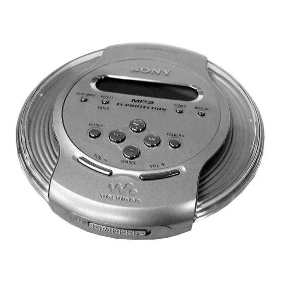
D-CJ01 SECTION 2 This section is extracted from GENERAL instruction manual. LOCATING THE CONTROLS CD player (front) Display SOUND button DISPLAY button REPEAT / ENTER button Strap holes 'm / M' (AMS / search) button PLAY MODE button FOLDER + button LINE OUT jack DC IN 4.5 V... -
Page 5: Disassembly
D-CJ01 SECTION 3 DISASSEMBLY The equipment can be removed using the following procedure. Cabinet (lower) sub ASSY MD mechanism Main board "Motor ASSY, Turn table (spindle) (M901)" Cabinet (inner) sub ASSY Switch unit "Motor ASSY (sled) (M902)", Optical pick-up (DAX-23E) Note : Follow the disassembly procedure in the numerical order given. -
Page 6: Main Board
D-CJ01 3-3. MAIN BOARD Cabinet (inner) sub ASSY 3 J301 2 J302 5 Flexble board Main board Cabinet (lower) sub ASSY 1 J401 3-4. “MOTOR ASSY, TURN TABLE 3-5. “MOTOR ASSY (SLED) (M902)”, (SPINDLE) (M901)” OPTICAL PICK-UP (DAX-23E) 1 Screws (B1.7x5) -
Page 7: Switch Unit
D-CJ01 3-6. SWITCH UNIT Lid (A) upper ASSY 5 Claws 5 Claws Switch unit Lid (B) upper ASSY 3 Screws 1 Screws 1 Screws Cabinet (inner) sub ASSY... -
Page 8: Electrical Adjustments
D-CJ01 SECTION 4 ELECTRICAL ADJUSTMENTS The CD section adjustments are done automatically in this set. Focus bias Check Condition: Precautions for Check • Hold the set in horizontal state. 1. Perform check in the order given. 2. Use YEDS-18 disc (Part No.: 3-702-101-01) unless otherwise Connection: indicated. -
Page 9: Diagrams
D-CJ01 SECTION 5 DIAGRAMS 5-1. EXPLANATION OF IC TERMINALS IC801 (SYSTEM CONTROL) µPD784216AY-CJ1 Pin No. Pin name Description — Not used (OPEN). 2 to 8 — — Not used (OPEN). — Power supply terminal. XTAL 0 Crystal oscillator output (8MHz). - Page 10 D-CJ01 AMUTE Audio mute signal output. VCC 2 ON HP amplifier ON/OFF output. XRST Reset terminal. WAKE UP Wakeup signal output. XLAT Latch signal output. 56 to 63 D 0 to D 7 LCD drive output. LCD drive output. 65 to 71 —...
-
Page 11: Block Diagram(1/2)
D-CJ01 5-2. BLOCK DIAGRAM (1/2) DVDD Q502 J301 IC603 LOUT2 XHGON LINE Q501 D0-3 A0-10 LOUT1 BUFFER BUFFER IC601 2,3,24,25 8-12,15-19,21 23 4 22 Q301 Q301 IC501 EFM DECODER,D/A, IC301 OPTICAL SERVO CONTROL RF AMP PICK-UP GAIN CTL HEADPHONE AMP... -
Page 12: Block Diagram(2/2)
D-CJ01 5-3. BLOCK DIAGRAM (2/2) (1/2) (1/2) D606 IC608 BUFFER XRDE_I LATCH LCD_RST_O XPOWLT_O DATA IC605 KEY2_AD KEY2 SDTO 63 64 12 13 14 KEY1_AD KEY1 SWITCH & DD0-7 DD0-7 IC604 UNIT IC801 (2/2) SYSTEM /WICK SCL0(I2C) CONTROL IC606 DQ1-3... -
Page 13: Printed Wiring Boards - Main Board (Side A)
D-CJ01 5-4. PRINTED WIRING BOARDS – MAIN BOARD (SIDE A) – : Uses unleaded solder. Semiconductor Location MAIN BOARD (SIDE B) Ref. No. Location Ref. No. Location CN801 D101 Q301 SWITCH D102 Q302 & D201 Q401 R666 D202 Q402 UNIT... -
Page 14: Printed Wiring Boards - Main Board (Side B)
D-CJ01 : Uses unleaded solder. 5-5. PRINTED WIRING BOARDS – MAIN BOARD (SIDE B) – Semiconductor MAIN BOARD (SIDE A ) Location Ref. No. Location D103 D203 D302 R668 D303 R664 D402 D403 SL602 D404 D407 OPTICAL PICK-UP D605 BLOCK... -
Page 15: Schematic Diagram - Main Section (1/4)
D-CJ01 5-6. SCHEMATIC DIAGRAM – MAIN SECTION (1/4) – Refer to page 20 to 21 for IC Block Diagrams. Refer to page 19 for Waveforms Refer to page 19 for Notes. -
Page 16: Schematic Diagram - Main Section (2/4)
D-CJ01 5-7. SCHEMATIC DIAGRAM – MAIN SECTION (2/4) – Refer to page 19 for Notes. -
Page 17: Schematic Diagram - Main Section (3/4)
D-CJ01 5-8. SCHEMATIC DIAGRAM – MAIN SECTION (3/4) – Refer to page 19 for Waveforms Refer to page 19 for Notes. -
Page 18: Schematic Diagram - Main Section (4/4)
D-CJ01 5-9. SCHEMATIC DIAGRAM – MAIN SECTION (4/4) – Refer to page 20 for IC Block Diagrams. Refer to page 19 for Waveforms Refer to page 19 for Notes. - Page 19 D-CJ01 Waveforms PLAY MODE 3.6Vp-p 3.8Vp-p 1.34 µsec 5.6 µ sec IC601 of Q411 C VOLT/DIV : 1 V AC VOLT/DIV : 1 V AC XTAO TIME/DIV : 20 nsec TIME/DIV : 2 µsec 30 Vp-p 0.4 - 0.8 Vp-p 8 MHz 0.125 µsec...
- Page 20 D-CJ01 IC Block Diagrams IC501 BA6779BFV-E2 IC301 TA2120FN (EL) BIAS MUTE MUTE BIAS BEEP AVDD BEEP BIAS OUT B OUT A IN2+ IV2- – – IN2- IV2+ IV3- IN3+ – – IN3- IV3+ RF IN OCL ROUT VREF LOUT RF BIAS...
- Page 21 D-CJ01 IC601 CXD3028R 120 119 118 117 116 115 114 113 112 111 110 109 108 107 106 105 104 103 102 101 100 99 98 97 96 95 94 93 92 91 ERROR CLOCK PCMD CORRECTOR GENERATOR SELECTOR LRCK...
-
Page 22: Exploded Views
D-CJ01 Ver 1.1 2002.01 SECTION 6 EXPLODED VIEWS NOTE : • -XX, -X mean standardized parts, so they • Abbreviation may have some difference from the original CND : Canadian The components identified by mark 0 or dotted line with mark one. -
Page 23: Main Section
D-CJ01 Ver 1.1 2002.01 6-2. MAIN SECTION Ref. No. Part No. Description Remark Ref. No. Part No. Description Remark X-3381-000-1 CABINET (LOWER) SUB ASSY (US) 4-223-609-01 KNOB (JOGGABLE) X-3381-001-1 CABINET (LOWER) SUB ASSY 4-908-792-61 SCREW (B2) (AEP,AUS,CH,CND,C&SA,EE,FR,KR,UK,JEW) 3-228-645-01 SPACER (MD) -
Page 24: Optical Pick-Up Section (Cdm-3123Eba)
D-CJ01 6-3. OPTICAL PICK-UP SECTION (CDM-3123EBA) M901 M902 The components identified by Les composants identifiés par mark 0 or dotted line with mark une marque 0 sont critiques 0 are critical for safety. pour la sécurité. Replace only with part number Ne les remplacer que par une specified. -
Page 25: Electrical Parts List
D-CJ01 Ver 1.1 2002.01 SECTION 7 ELECTRICAL PARTS LIST MAIN NOTE : • Due to standardization, replacements in the • SEMICONDUCTORS In each case, u : µ , for example : The components identified by mark 0 parts list may be different from the parts uA.. - Page 26 D-CJ01 MAIN Ref. No. Part No. Description Remark Ref. No. Part No. Description Remark C447 1-162-970-11 CERAMIC CHIP 0.01uF C651 1-164-156-11 CERAMIC CHIP 0.1uF C448 1-104-752-11 TANTAL. CHIP 33uF 6.3V C652 1-164-156-11 CERAMIC CHIP 0.1uF C449 1-162-970-11 CERAMIC CHIP 0.01uF...
- Page 27 D-CJ01 MAIN Ref. No. Part No. Description Remark Ref. No. Part No. Description Remark D411 8-719-404-50 DIODE MA111-TX L408 1-414-434-11 INDUCTOR 100uH D412 8-719-072-70 DIODE MA2ZD14001S0 L409 1-414-402-11 INDUCTOR 47uH D413 8-719-422-37 DIODE MA8051 L410 1-419-188-41 INDUCTOR 100uH D602 8-719-044-74 DIODE MA792WK-TX...
- Page 28 D-CJ01 MAIN Ref. No. Part No. Description Remark Ref. No. Part No. Description Remark R207 1-216-813-11 METAL CHIP 1/16W R208 1-216-821-11 METAL CHIP 1/16W R450 1-216-841-11 METAL CHIP 1/16W R209 1-218-867-11 RES-CHIP 6.8K 1/16W R451 1-216-864-11 METAL CHIP 1/16W R452 1-216-825-11 METAL CHIP 2.2K...
- Page 29 D-CJ01 MAIN Ref. No. Part No. Description Remark Ref. No. Part No. Description Remark R628 1-216-839-11 METAL CHIP 1/16W R629 1-216-851-11 METAL CHIP 330K 1/16W R807 1-216-839-11 METAL CHIP 1/16W R630 1-216-857-11 METAL CHIP 1/16W R808 1-216-845-11 METAL CHIP 100K...
- Page 30 D-CJ01 Ver 1.1 2002.01 Ref. No. Part No. Description Remark ACCESSORIES *********** 1-475-622-21 ADAPTOR, AC (AC-E455) (CH) 1-476-395-12 REMOTE CONTROL UNIT (EXCEPT US,CND) 1-476-739-11 ADAPTOR, AC (AC-E455) (KR) 1-476-845-11 ADAPTOR, AC (AC-ES455) (AEP,E13,EE,FR) 1-476-846-11 ADAPTOR, AC (AC-ES455) (HK) 1-476-848-11 ADAPTOR, AC (AC-ES455) (UK) 1-476-850-11 ADAPTOR, AC (AC-ES455) (AUS) 1-476-851-11 ADAPTOR, AC (AC-ES455) (CND,C&SA,US)
- Page 31 D-CJ01...
- Page 32 D-CJ01 REVISION HISTORY Clicking the version allows you to jump to the revised page. Also, clicking the version at the upper right on the revised page allows you to jump to the next revised page. Ver. Date Description of Revision 2002.01...
Need help?
Do you have a question about the D-CJ01 and is the answer not in the manual?
Questions and answers