Advertisement
Quick Links
Advertisement

Summary of Contents for BK Precision 501A
- Page 1 Semiconductor · Curve Tracer •...
- Page 2 Dear Friend: Congratulations on your purchase of B & K - Precision Test Equipment, and welcome to the B & K family. We hope your experience with your new test equip ment will make you a lifetime B & K customer. Your instrument is backed by more than 20 years of experience in designing and manufacturing.
- Page 5 B & K PRECISION MODEL 501-A PARTS LIST B & K PRECISION MODEL 501-A PARTS LIST 488-113-9-002 8 SCHEMATIC B&K B&K SCHEMATIC SYMBOL DESCRIPTION PART No. SYMBOL DESCRIPTION PART No. TRANSFORMERS CAPACITORS Power Transformer, 117V AC Primary ....065-067-9-001 C-1, 2 1000 µ.fd, 35 Volt Electrolytic Capacitor .....
- Page 6 lt!OTE -IT<ILUS Ofl(tllWIS( Y1:C.ir1(� " lCZ•P<.'i >-�'I. PIN 7 T(l-(lf!O Ill'! :. 1/<IW, lttSISTCfll P�,(AGL Vllt.1.€S V,Sl V$.l0 IC)l!l!C4-11,'><I ro .. ,v. 11\NIIT()� l:l!fi 6-CCMW()ll); "' Ml>'o • C• PINI -�II l'!!';:0-:61( l'IN 1i-1:o; ,�., , ( l .tu 111($1$10 1 1$ ., ..$-X.. WU,($ S"(�t·,rn IN 0,!MS I)"...
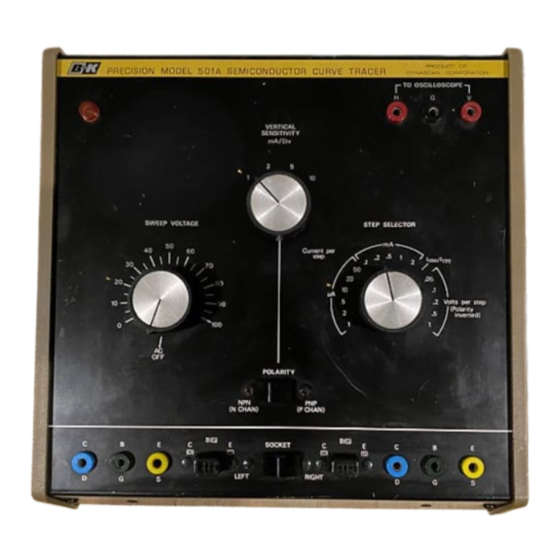
- Page 8 Figure 1. Controls and Operator's Facilities...
- Page 9 CONTROLS AND OPERATOR'S FACILITIES 1. Pilot Lamp 9. E,S Terminal Lights when unit is on. Connection emitter source of semiconductor to tested. Active when 2. SWEEP Combination on-off switch SOCKET switch is in RIGHT VOLTAGE and sweep voltage control. position. Control [n the completely counter...
- Page 14 Curve Tracer Oscilloscopt: Connections to Test leads connecting the curve tracer to the os cilloscope should be set-up as follows: CURVE TRACER OSCILLOSCOPE Place 9ratlcule over screen, cut to size V jack ... Vertical Input II neceuary. H jack ... Horizontal Input G jack ...
- Page 15 of the curve tracer front panel. Either set of jacks TRACER SUPPLIES THE COMPLETE TEST SIGNAL. ANY ADDITIONAL SIGNAL OR may be used. The SOCKET switch activates only DC CURRENT MAY INVALIDATE THE the left or right set of jacks at a given time, along TEST RESULTS AND COULD RESULT IN with the respective plug-in socket.
- Page 19 single curve appears on the screen opposite to where normal curves appear. This represents base-emitter breakdown voltage of the device under test. Matching two complementary devices may be ac complished by inserting the PNP unit in the right left socket and the NPN unit in the socket.
- Page 20 as insufficient gain to be detected. Until equipment reference files of normal waveform displays. For manufacturers begin to supply such information on shops which specialize in servicing a specific brand their schematics or servicing diagrams, servicemen of solid state products, the time required to produce must rely on the go no-go test or develop their own a reference file may be well worthwhile.
- Page 21 DC Current Gain (DC beta) calculate DC beta even though none of the curves The DC or s�atic current gain of a transistor is pass through the measurement point. Simply approx defined as the ratio of collector current to base cur imate the percentage of distance between the curves rent measured at one specific point of collector volt...
- Page 24 6 mA, a 2mA change. As it swings negatively to operation. The transistor will operate with a load, 10 p,A (1st curve), the collector current decreases not at a specific fixed V The load causes operation 0 • for 4 mA to 2.1 mA, a 1.9 mA change. Out of the along the load line, since an increase in collector current will reduce collector voltage and vice versa.
- Page 25 LEAKAGE MEASUREMENT (lcEo) Collector leakage current is the collector-to-emitter current that flows when the transistor is supposed -CURRENT to be completely off. If the transistor is leaky, in creasing collector voltage causes the collector cur rent to increase independently of the base current. .
- Page 27 (Figure 25C). The entire family of curves moves in LOOP IN CURVES the direction of higher collector current as the tem perature build-up continues. This regenerative or "runaw " phenomena may easily destroy the transistor if not stopped immediately. CAUTION Testing procedures should not be con...
- Page 28 2. Plug the FET to be tested into either of the increased after the FET is inserted only as much as sockets of the curve tracer, or be con is necessary to make the tests. Some MOS FET's nected to the D, G and S jacks with test leads. can be damaged by a voltage transient from a static Use the FET manufacturer's basing diagram, if charge carried by the person handling the device.
- Page 29 As with NPN and PNP transistors, the gain of a t.Io FET is not constant over its entire voltage and cur g m = at a given drain voltage rent range. The gain is normally calculated in its t.VG typical operating range. Distortion and linearity may be determined by the same method as desribed t:N G 10.2v - o .1v1 for transistors;...
- Page 31 shown in Figure 29. Note: Refer to To obtain the most accurate voltage reading pos "Breakdown Voltage Measurement" if the oscilloscope being used sible, calibrate the full scale oscilloscope horizontal has less than 1 Mn of horizontal input impedance. sensitivity to a convenient value slightly above the Zener voltage.
- Page 32 TESTING UNIJUNCTION TRANSISTORS A unijunction transistor (UJT), as the name im appear quite close together and careful observation plies, is a single junction device possessing three may be required to distinguish the individual curves. terminals. Conduction from base l to base 2 is It may be helpful to "spread out"...
- Page 33 Reverse blocking voltage is normally higher than place the SCR in the "on" condition. forward blocking voltage. The Model 501A can measure reverse blocking voltage up to 100 volts. The forward voltage drop during the "on" condi...
-
Page 34: Schematic Representation
range of voltage vs current. Read the forward volt the SCR. Otherwise, the curve tracer is set up as for age drop directly from the displ forward blocking voltage measurement. Two types Gate Trigger Voltage (Figure 35) of measurements can be made: The "turn on"... -
Page 36: Maintenance And Calibration
7. Turn the AC power on and adjust the ZERO trim 4. Attach a digital voltmeter to TP29 and turn on mer on the 501A PC board until the DC voltmeter A C power to the unit. reads "O". Remove temporary short from TP29. -
Page 37: Troubleshooting
to follow the explicit control setting and set-up pro For displaying 7 curves, it is necessary to add a cedure as given in the "notes" column in order to third diode. Any general purpose germanium device obtain the illustrated waveforms. Point-by-point sig is acceptable. -
Page 38: Circuit Description
CIRCUIT DESCRIPTION The B & K Model 501A utilizes a total of 8 inte to a countdown chain composed of 3 flip-flops within grated circuits for an equivalent discrete transistor two IC packages (IC3 and 4). The second flip-flop of count of 204 devices. - Page 39 linked together forming an accurate constant-current former is full-wave rectified by a diode bridge (DI source for driving bipolar transistors. through D4) to produce a 120Hz "sweep" signal. No The precise voltage staircase from ICS is injected capacitance filtering is used in order to retain fidel into either the non-inverting or inverting input of ity of the positive half sine-waves.
-
Page 40: Warranty
WARRANTY SERVICE INSTRUCTIONS 1. Refer to the maintenance section of the instruction manual for adjust ments that may be applicable. 2. Check common electronic parts such as tubes, transistors and batteries. Always check instruction manual for applicable adjustments after such replacement.
Need help?
Do you have a question about the 501A and is the answer not in the manual?
Questions and answers