Samsung HT-F4500 Service Manual
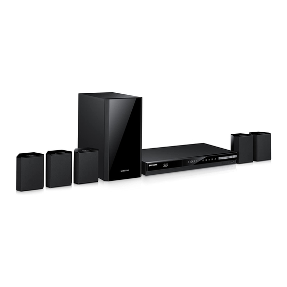
5.1ch blu-ray™ home entertainment system
Hide thumbs
Also See for HT-F4500:
- User manual (152 pages) ,
- Features (2 pages) ,
- User manual (75 pages)
Table of Contents
Advertisement
SERVICE
5.1CH Blu-ray™ Home
Entertainment System
HT-F4500
Refer to the service manual in the GSPN (see the rear cover) for more information.
5.1CH Blu-ray™ Home
Entertainment System
Model Name
Model Code
MANUAL
1. Precaution
2. Product Specification
3. Disassembly and Reassembly
4. Troubleshooting
5. PCB Diagram
6. Schematic Diagram
HT-F4500
HT-F4500/EN
Contents
Advertisement
Table of Contents

Related Manuals for Samsung HT-F4500


Summary of Contents for Samsung HT-F4500
- Page 1 5.1CH Blu-ray™ Home Entertainment System Model Name HT-F4500 Model Code HT-F4500/EN SERVICE MANUAL 5.1CH Blu-ray™ Home Contents Entertainment System 1. Precaution 2. Product Specification 3. Disassembly and Reassembly 4. Troubleshooting HT-F4500 5. PCB Diagram 6. Schematic Diagram Refer to the service manual in the GSPN (see the rear cover) for more information.
-
Page 2: Table Of Contents
FRONT PCB Bottom ....................... 5 − 5 5.4. MAIN PCB Top ........................5 − 6 5.4.1. Pin Connection ......................5 − 7 5.4.2. Test Point Wave Form ....................5 − 8 5.5. MAIN PCB Bottom........................5 − 9 Copyright© 1995-2012 SAMSUNG. All rights reserved. - Page 3 6.11. F/E-2............................. 6 − 13 6.12. FRONT MICOM ........................6 − 14 6.13. PWM ............................ 6 − 15 6.14. AMP ............................. 6 − 16 6.15. SMPS-1 ..........................6 − 17 6.16. SMPS-2 ..........................6 − 18 Copyright© 1995-2012 SAMSUNG. All rights reserved.
-
Page 4: Precaution
TES T ALL EXPO SED METAL SU RFACES 2-WIRE C ORD ALSO TES T WITH PLUG REVER SE D (US ING AC EARTH ADAPTER PLUG GROUND AS R EQ UIRED) Figure 1.1 AC Leakage Test Copyright© 1995-2012 SAMSUNG. All rights reserved. - Page 5 Use replacement components that have the same ratings, especially for flame resistance and dielectric strength specifications. A replacement part that does not have the same safety characteristics as the original might create shock, fire or other hazards. Copyright© 1995-2012 SAMSUNG. All rights reserved.
-
Page 6: Servicing Precautions
CAUTION First read the “Safety Precautions” section of this manual. If some unforeseen circumstance creates a conflict between the servicing and safety precautions, always follow the safety precautions. Copyright© 1995-2012 SAMSUNG. All rights reserved. -
Page 7: Precautions For Electrostatically Sensitive Devices (Esds)
8) Minimize body motions when handling unpackaged replacement ESDs. Motions such as brushing clothes together, or lifting a foot from a carpeted floor can generate enough static electricity to damage an ESD. Copyright© 1995-2012 SAMSUNG. All rights reserved. -
Page 8: Product Specification
DTS-HD Master Audio decoding from the beginning of the Mass Production. • MP3, MKV, MP4, WMA, WMV • Support 11 CP (Netflix, Pandora, CinemaNow, Vudu., etc) • 1 USB port (Front) • Support 3D Disc • HDMI 1.4 with ARC • DLNA Copyright© 1995-2012 SAMSUNG. All rights reserved. -
Page 9: Specifications
Amplifier Analog input 20 Hz ~ 20 kHz (±3 dB) Frequency response Digital input 20 Hz ~ 40 kHz (±4 dB) S/N Ratio 70 dB Channel separation 60 dB (AUX) 500 mV Input sensitivity Copyright© 1995-2012 SAMSUNG. All rights reserved. - Page 10 200 W Dimensions 6.10 x 11.81 x 3.03 x 4.25 x 2.75 3.03 x 4.25 x 2.75 8.97 x 3.03 x 2.75 (W x H x D) (inches) 11.22 0.78 0.84 1.08 6.36 Weights (Ibs) Copyright© 1995-2012 SAMSUNG. All rights reserved.
-
Page 11: Specifications Analysis
Front Micom RENESAS SANYO MAIN Chip BROADCOM Wi-Fi LAN Dongle HDMI IN BACKEND MTK BACKEND BROADCOM Main ↔ Loader (Loader : included MTK) (Loader : included BROADCOM) O : Feature Included X : Not Included Copyright© 1995-2012 SAMSUNG. All rights reserved. -
Page 12: Accessories
2. Product Specification 2.4. Accessories 2.4.1. Supplied Accessories Accessories Item Item code Remote Control AH59-02530A Batteries (AAA size) 4301-000116 Power Cable 3903-000525 FM Antenna AH42-00021A AH68-02574M User’s Manual AH68-02574N Copyright© 1995-2012 SAMSUNG. All rights reserved. -
Page 13: Disassembly And Reassembly
Disconnect 2 FFC cables from deck and SMPS wire and fan wire and FFC cable from front assy. Unfasten 3 screws on the Main PCB. : BH,+,B,M3,L6,ZPC(WHT),SWRCH18A 3 screws on the back side. : BH,+,B,M3,L10,ZPC(BLK),SWRCH18A Copyright© 1995-2012 SAMSUNG. All rights reserved. - Page 14 Up and away from the device. The 4 hooks on the top will be loosened as you lift the FRONT-COVER from the bottom. Unfasten 3 screws on the Front PCB. : BH,+,B,M3,L10,ZPC(BLK),SWRCH18A Copyright© 1995-2012 SAMSUNG. All rights reserved.
- Page 15 3. Disassembly and Reassembly Description Description Photo 10. Unfasten the Assy-Deck by pushing the locking points on the side. 11. Unfasten 5 screws on the SMPS. Copyright© 1995-2012 SAMSUNG. All rights reserved.
- Page 16 3. Disassembly and Reassembly Description Description Photo 12. Unfasten 3 screws on the back side. : BH,+,B,M3,L10,ZPC(BLK),SWRCH18A) Remove the SMPS and Fan. Copyright© 1995-2012 SAMSUNG. All rights reserved.
-
Page 17: Troubleshooting
4. Troubleshooting 4. Troubleshooting 4.1. Checkpoints by Error Mode Oscilloscope Setting Values Normal Voltage 24 MHz 32.768 KHz Voltage/DIV 1 V/div 200 mV/div 500 mV/div TIME/DIV 100 ms/div 100 ns/div 100 us/div Copyright© 1995-2012 SAMSUNG. All rights reserved. -
Page 18: No Power
CN21 #11, #12 pin Cha nge S MP S . 3.4V is OK? Ye s Does CN21 Cha nge S MP S . #6, #7, #8 pin have 12V? Ye s Cha nge MAIN P CB. Copyright© 1995-2012 SAMSUNG. All rights reserved. -
Page 19: No Audio
I2S line s a nd output No s ound a t a ll cha nne ls ? Change M AIN PCB. block ha ve proble ms ? (soldering etc...) Ye s Ye s Change MAIN PCB. Re-soldering problem's components. Copyright© 1995-2012 SAMSUNG. All rights reserved. -
Page 20: Disc Loading Error
Fro nt End P owe rs Cha nge MAIN P CB. (12V, 5V, 3.3V) a re OK? Ye s Cha nge MAIN P CB. Is SP IN Motor working? Ye s Cha nge De ck. Copyright© 1995-2012 SAMSUNG. All rights reserved. -
Page 21: Remote Doesn't Work
Re fe r to wa ve pa tte rn Ye s ima ge of Fig. 4-1. Cha nge FRONT P CB. Cha nge Re mote Control. Copyright© 1995-2012 SAMSUNG. All rights reserved. - Page 22 DGND V_GND V_GND 40000OHM 40000OHM DGND DGND R_EYE R_EYE DGND DGND DGND DGND V_GND V_GND 40000OHM 40000OHM * 6.2. FRONT <Re mote Eye Da ta > * 5.2. FRONT P CB Top <Fig. 4-1> Copyright© 1995-2012 SAMSUNG. All rights reserved.
-
Page 23: No Image On Screen
IC1's re s ona tor(X376)'s cha nge this , cha nge MAIN P CB. clock is ok? Re fe r to wa ve pa tte rn ima ge of Fig. 4-3. Ye s Change MAIN PCB. Copyright© 1995-2012 SAMSUNG. All rights reserved. - Page 24 MGND3 MGND1 MGND1 DGND DGND DGND DGND HD3107 HD3107 DGND DGND ARC_DATA+ ARC_DATA+ * 6.4. HDMI/ARC <HDMI EYE S IGNAL> IC 3 1 N 1 6 * 5.4. MAIN P CB Top <Fig. 4-2> Copyright© 1995-2012 SAMSUNG. All rights reserved.
- Page 25 AVSS3 3_VDAC AVSS3 3_VDAC AOSDATA1 AOSDATA1 D3.3V_PW D3.3V_PW AOSDATA0 AOSDATA0 R166 R166 33OHM 33OHM 1/16W 1/16W AOLRCK AOLRCK * 6.4. HDMI/ARC <X3 Mus t be 27MHz> * 5.4. MAIN P CB Top <Fig. 4-3> Copyright© 1995-2012 SAMSUNG. All rights reserved.
-
Page 26: Disc Skips Or Freezing
Cha nge De ck. On ly DVD NG? ha ve proble m? Re -s olde ring SQ10. Doe s S Q8 Cha nge De ck. ha ve proble m? Re -s olde ring SQ8. 4-10 Copyright© 1995-2012 SAMSUNG. All rights reserved. -
Page 27: No Disc Reading Error
Ele ctronic s s e rvice . on the Sa msu ng We b Site ? Ye s Upda te to the ne w ve rs ion firmwa re a nd try aga in. Copyright© 1995-2012 SAMSUNG. All rights reserved. 4-11... -
Page 28: Network Error
The connection between LAN and SET is direct. So there is no need to check H/W if there is network problem. If it is, the problem is MAIN CHIP (IC1)'s BGA soldering problem. It must be changed to a new board. 4-12 Copyright© 1995-2012 SAMSUNG. All rights reserved. -
Page 29: Initialization & Upgrade Methods
Support→ Contact Samsung • Description for the meaning Front : System micom S/W : BACKEND Firmware Loader : Loader Firmware Region : BD region code / DVD region code Model : Model name Copyright© 1995-2012 SAMSUNG. All rights reserved. 4-13... -
Page 30: How To Update Firmware
• Never turn the product off or on manually during the update process. • Samsung Electronics takes no legal responsibility for a product malfunction caused by an unstable internet connection or consumer negligence during software upgrade. 4-14 Copyright© 1995-2012 SAMSUNG. All rights reserved. - Page 31 Never turn the product on or off manually during the update process. • Samsung Electronics shall take no legal responsibility for product malfunction caused by unstable of internet connection or consumer negligence during software upgrade. Copyright© 1995-2012 SAMSUNG. All rights reserved.
-
Page 32: Cold Start Method (Initialize Setup)
※ ※ ※ Method 1) Press “■” button on the front panel for over 5 seconds while ‘no disc’ status. 2) Then, VFD sign : “INIT” → Power will be turned off automatically. 4-16 Copyright© 1995-2012 SAMSUNG. All rights reserved. -
Page 33: Buyer-Region Code Setting Method
4) The VFD will now say TEST – – , now insert 46. 5) The VFD will now read – – –. Insert the correct Region code based on the table below. Ex: For USA Buyers you will type in 0 2 0. Copyright© 1995-2012 SAMSUNG. All rights reserved. 4-17... - Page 34 SINGAPORE, VIETNAM (XS), INDONESIA (XD), MALAYSIA (XM), THAILAND (XT), Philippine (XP) CHINA (XZ) HONGKONG (ZK), TAIWAN (ZW) KOREA (KR) IRAN (HC), Arab-Emirate (D), Jordan (J), Tunis (H), Egypt, Iraq, Syria, Lebanon, Israel, Algeria, Saudi Arabia Ethiopia, South Africa, Nigeria, Kenya, Sudan 4-18 Copyright© 1995-2012 SAMSUNG. All rights reserved.
-
Page 35: Pcb Diagram
5. PCB Diagram 5. PCB Diagram 5.1. Wiring Diagram DECK S MP S FRONT MAIN Copyright© 1995-2012 SAMSUNG. All rights reserved. -
Page 36: Front Pcb Top
5. PCB Diagram 5.2. FRONT PCB Top VC N 5 FCON1 Copyright© 1995-2012 SAMSUNG. All rights reserved. -
Page 37: Pin Connection
5. PCB Diagram 5.2.1. Pin Connection 1) FCON1 VFD/REMOTE Control IR Pin No. Signal USB5V_1 USB5V DGND USB- USB+ DGND REMO DGND ST3.4V DGND DGND VFDCE VFDDATA VFDCLK DGND TACT DGND Copyright© 1995-2012 SAMSUNG. All rights reserved. -
Page 38: Test Point Wave Form
5. PCB Diagram 5.2.2. Test Point Wave Form Copyright© 1995-2012 SAMSUNG. All rights reserved. -
Page 39: Front Pcb Bottom
5. PCB Diagram 5.3. FRONT PCB Bottom Copyright© 1995-2012 SAMSUNG. All rights reserved. -
Page 40: Main Pcb Top
5. PCB Diagram 5.4. MAIN PCB Top CN12 CN94 UIC 3 WC N 1 IC 1 UIC1 IC 6 IC3 1 IC 31 IC 2 2 AIC 2 AIC 2 AIC 3 IC 22 01 CN21 Copyright© 1995-2012 SAMSUNG. All rights reserved. -
Page 41: Pin Connection
GND_1 TPIC_CO_A- DGND TPIC B+ ST3.4V_1 TPIC_CO_B+ TPIC_MICOM ST3.4V_2 TPIC_CO_B- TPIC_U TPIC_V DGND VARI TPIC_W VFDCE PGND4 VFDDATA PGND3 VFDCLK PGND2 DGND PGND1 TACT +35V_5 RFO- DGND +35V_4 RFO+ +35V_3 +35V_2 FD5.0V_PW +35V_1 GAINSW1 Copyright© 1995-2012 SAMSUNG. All rights reserved. -
Page 42: Test Point Wave Form
5. PCB Diagram 5.4.2. Test Point Wave Form Copyright© 1995-2012 SAMSUNG. All rights reserved. -
Page 43: Main Pcb Bottom
5. PCB Diagram 5.5. MAIN PCB Bottom IC414 Copyright© 1995-2012 SAMSUNG. All rights reserved. -
Page 44: Smps Pcb Top
5. PCB Diagram 5.6. SMPS PCB Top CNM80 5-10 Copyright© 1995-2012 SAMSUNG. All rights reserved. -
Page 45: Pin Connection
5. PCB Diagram 5.6.1. Pin Connection 1) CNM801 Power Connector Pin No. Signal VF+_2 VF-_2 VP_2 GND_3 D12V_2 D12V_1 D12V_3 GND_2 GND_1 ST3.4V_1 ST3.4V_2 VARI PGND4 PGND3 PGND2 PGND1 +35V_5 +35V_4 +35V_3 +35V_2 +35V_1 Copyright© 1995-2012 SAMSUNG. All rights reserved. 5-11... -
Page 46: Smps Pcb Bottom
5. PCB Diagram 5.7. SMPS PCB Bottom 5-12 Copyright© 1995-2012 SAMSUNG. All rights reserved. -
Page 47: Schematic Diagram
Buffe r • HT-F4500 model supports 1 USB port. It is for USB file play like MP3, JPG and etc. • About MT8560 Audio output, I2S datas go PWM IC(TAS5538) to convert PWM signals and then go to AMP IC (TAS5614). -
Page 48: Front
REMO REMO DGND_3 DGND_3 AL3.3V AL3.3V VGND_1 VGND_1 VGND_2 VGND_2 VFD_CE VFD_CE VFD_CE VFD_CE VFD_DATA VFD_DATA VFD_DATA VFD_DATA VFD_CLK VFD_CLK VFD_CLK VFD_CLK VGND_3 VGND_3 TACT_KEY TACT_KEY TACT_KEY TACT_KEY DGND_4 DGND_4 V_GND V_GND DGND DGND Copyright© 1995-2012 SAMSUNG. All rights reserved. -
Page 49: Test Point Wave Form
6. Schematic Diagram 6.2.1. Test Point Wave Form Copyright© 1995-2012 SAMSUNG. All rights reserved. -
Page 50: Dc-Dc Power
R18 6 R186 DGND DGND DGND DGND R12V R12V B12V_PW B12V_PW UNDEFINED UNDEFINED DGND DGND DGND DGND 0.01OHM 0.01OHM DGND DGND CB2012UA300T CB2012UA300T BD22 BD22 FE12V_PW FE12V_PW UNDEFINED UNDEFINED 0.01OHM 0.01OHM CB2012UA300T CB2012UA300T BD94 BD94 Copyright© 1995-2012 SAMSUNG. All rights reserved. -
Page 51: Dir/Adc/Video
100K OHM 47UF 47UF 22P F 22P F 1/16W 1/16W R873 R873 1/16W 1/16W 12KO HM 12KO HM C126 C126 1MOHM 1MOHM 12. 288M HZ 12. 288M HZ DGND DGND DGND DGND DGND DGND Copyright© 1995-2012 SAMSUNG. All rights reserved. -
Page 52: Hdmi/Arc
DGND DGND HR316 HR316 82PF 82PF DGND DGND HDMI_CEC HDMI_CEC HQ3 10 HQ3 10 ARC_DATA+ ARC_DATA+ DGND DGND HC4005 HC4005 HR409 HR409 HDMI_CEC_M ICOM HDMI_CEC_M ICOM ARC_DATA- ARC_DATA- 0OHM 0OHM MICOM MICOM HC4006 HC4006 Copyright© 1995-2012 SAMSUNG. All rights reserved. -
Page 53: Test Point Wave Form
6. Schematic Diagram 6.5.1. Test Point Wave Form Copyright© 1995-2012 SAMSUNG. All rights reserved. -
Page 54: Nand/Ethernet/Usb
RX_SD 0 VOUTD15 VOUTD15 100OHM 100OHM 1/16W 1/16W DIR_INT1 DIR_INT1 VOUTHSYNC VOUTHSYNC REXT REXT 1/16W 1/16W VOUTVSYNC VOUTVSYNC VVSYNC VVSYNC 24KOHM 24KOHM FAST_EJE CT FAST_EJE CT VOUTCLK VOUTCLK R444 R444 DGND DGND DGND DGND Copyright© 1995-2012 SAMSUNG. All rights reserved. -
Page 55: Ddr3 Bank#0
DGND12_K DGND12_K D1.5V_PW D1.5V_PW DGND12_K DGND12_K DGND12_K DGND12_K DGND12_K DGND12_K DGND DGND DGND DGND D1.5V_PW D1.5V_PW D1.5V_PW D1.5V_PW D1.5V_PW D1.5V_PW DDR3_0.75V_VREF0_PW DDR3_0.75V_VREF0_PW DDR3_0.75V_VREF0_PW DDR3_0.75V_VREF0_PW DGND DGND DGND DGND DGND DGND DGND DGND DGND DGND Copyright© 1995-2012 SAMSUNG. All rights reserved. -
Page 56: Ddr3 Bank#1
DDR3_CLK23- _CLK DDR3_CLK23- _CLK RCLK0__B RCLK0__B DDR3_0. 75V_VREF0_P W DDR3_0. 75V_VREF0_P W RVREF0_B RVREF0_B C619 C619 100NF 100NF DGND DGND DGND DGND D1.5V_PW D1.5V_PW D1.2V_PW D1.2V_PW DDR3_0.75V_VREF0_PW DDR3_0.75V_VREF0_PW DGND DGND DGND DGND DGND DGND 6-10 Copyright© 1995-2012 SAMSUNG. All rights reserved. -
Page 57: Misc/Uart/Strap
[ 1, 0, X] : OLT M ODE [ 1, 0, X] : OLT M ODE NFREN NFREN [ 0, 1, X] : ABI ST M ODE [ 0, 1, X] : ABI ST M ODE DG ND DG ND Copyright© 1995-2012 SAMSUNG. All rights reserved. 6-11... - Page 58 CLOSE TO 8551 IC PAD TPIC_FR+ TPIC_FR+ DGND DGND TPIC_TR+ TPIC_TR+ TPIC_TR- TPIC_TR- TPIC_TILT- TPIC_TILT- TPIC_TILT+ TPIC_TILT+ MGND2 MGND2 MGND4 MGND4 TPIC_FR- TPIC_FR- TPIC_FR+ TPIC_FR+ TPIC_TR+ TPIC_TR+ DGND DGND PU_SELE CT PU_SELE CT DGND DGND DGND DGND 6-12 Copyright© 1995-2012 SAMSUNG. All rights reserved.
- Page 59 C938 TPIC_B- TPIC_B- TPIC_A+ TPIC_A+ TPIC_COMMON TPIC_COMMON TP13 TP13 TPIC_A- TPIC_A- TPIC_U TPIC_U TP14 TP14 TPIC_V TPIC_V TP15 TP15 TPIC_W TPIC_W TP16 TP16 C937 C937 DGND DGND DGND DGND AGND AGND AGND AGND Copyright© 1995-2012 SAMSUNG. All rights reserved. 6-13...
-
Page 60: Front Micom
F_R ES ET F_R ES ET T_OGN D T_OGN D AL3.3V_PW AL3.3V_PW NO USE NO USE MICOM_RESET MICOM_RESET /RESE T,RE SE T /RESE T,RE SE T UIC2 UIC2 CAT853STBI-G T3 CAT853STBI-G T3 DGND DGND 6-14 Copyright© 1995-2012 SAMSUNG. All rights reserved. -
Page 61: Pwm
BD11 0.01OHM 0.01OHM 0.01OHM 0.01OHM 5000MA 5000MA OPTION OPTION DGND DGND 5000MA 5000MA FGND FGND Q201 Q201 TP1202 TP1202 KRC106S- RTK KRC106S- RTK OPTION OPTION KRC106S- RTK KRC106S- RTK Q202 Q202 DGND DGND Copyright© 1995-2012 SAMSUNG. All rights reserved. 6-15... -
Page 62: Amp
PGND 100NF 100NF 100NF 100NF PGND PGND 100NF 100NF 0.01OH M 0.01OH M PGND PGND PGND PGND DGND DGND DGND DGND PGND PGND PGND PGND DGND DGND PGND PGND PGND PGND PGND PGND 6-16 Copyright© 1995-2012 SAMSUNG. All rights reserved. -
Page 63: Smps-1
S OD-123 CN801S RS 817 1K(1608) 0721-6-PP4 RS 818 P C802S QS 804 LTV817(B) 2N7002 RS 819 P S -ON S OT-23 20K(1608) P -GND RS 820 CS 827 150K(1608) 0.01uF(1608) S -GND Copyright© 1995-2012 SAMSUNG. All rights reserved. 6-17... -
Page 64: Smps-2
1K(1608) ZDS 809 A3.4V DM805 QS 812 BAV70 2N7002 4.3V,S OD-123 S OT-23 ZDS 808 B12V RS 843 1M(1608) 15V,S OD-123 RM821 RS 837 RS 836 DM806 1K(1608) 1K(1608) 1K(1608) BAV70 S -GND 6-18 Copyright© 1995-2012 SAMSUNG. All rights reserved. - Page 65 E.Asia, W.Asia, https://gspn2.samsungcsportal.com China, Japan N.America, S.America https://gspn3.samsungcsportal.com This Service Manual is a property of Samsung Electronics Co.,Ltd. © 2012 Samsung Electronics Co.,Ltd. Any unauthorized use of Manual can be punished under All rights reserved. applicable International and/or domestic law.
Need help?
Do you have a question about the HT-F4500 and is the answer not in the manual?
Questions and answers