
Summary of Contents for rtd DM34116HR
- Page 1 DM34116HR 1-25MHz A/D Digitizer with 25Mhz D/A Outputs User’s Manual BDM-610010057 Rev A RTD Embedded Technologies, Inc. AS9100 and ISO 9001 Certified...
- Page 2 RTD Embedded Technologies, Inc. 103 Innovation Boulevard State College, PA 16803 USA Telephone: 814-234-8087 Fax: 814-234-5218 www.rtd.com sales@rtd.com techsupport@rtd.com DM34116HR | www.rtd.com User’s Manual RTD Embedded Technologies, Inc. BDM-610010057 Rev A...
- Page 3 Failure to follow the instructions found in this manual may result in damage to the product described in this manual, or other components of the system. The procedure set forth in this manual shall only be performed by persons qualified to service electronic equipment. Contents and specifications within this manual are given without warranty, and are subject to change without notice. RTD Embedded Technologies, Inc. shall not by persons qualified to service electronic equipment.
-
Page 4: Table Of Contents
Analog input ....................................29 5.8.1 Initializing the ADC Converter 5.8.2 Simplified block diagram of analog input 5.8.3 Input connection examples Analog Output ................................... 32 5.9.1 Initializing the DAC Converter DM34116HR | www.rtd.com User’s Manual RTD Embedded Technologies, Inc. BDM-610010057 Rev A... - Page 5 6.4.15 ADC_TRIM (Read/Write) 6.4.16 ADC_TRIM_BUSY (Read Only) 6.4.17 FRONT_END_CONFIG (Maskable Read/Write) 6.4.18 FIFO_DATA_CNT (Read) 6.4.19 MAX_FIFO_SIZE (Read) 6.4.20 FILTER (Read/Write) 6.4.21 INT_STAT(Read/Clear) 6.4.22 INT_ENA (Read/Write) 6.4.23 THRESH_LOW (Read/Write) DM34116HR | www.rtd.com User’s Manual RTD Embedded Technologies, Inc. BDM-610010057 Rev A...
- Page 6 6.1.2 Mode_Status (Read/Write, Read-Only) 6.1.3 CLK_SRC (Read/Write) 6.1.4 START_TRIG (Read/Write) 6.1.5 STOP_TRIG (Read/Write) 6.1.6 CLK_DIV (Read/Write) 6.1.7 CLK_DIV_CNTR (Read Only) 6.1.8 PERIOD_COUNT (Read Only) 6.1.9 INT_ENA (Maskable Read/Write) DM34116HR | www.rtd.com User’s Manual RTD Embedded Technologies, Inc. BDM-610010057 Rev A...
- Page 7 CONFIG (Maskable Read/Write) 6.6.12 DELAY_COUNTER_n (Read/Write) 6.6.13 CAPTURE_COUNTER_n (Read/Write) BAR2: SyncBus ..................................73 6.7.1 Function Block Register Map 6.7.2 CLK_SEL (Read) 6.7.3 PLL_LOCKED (Read Only) 6.7.4 TERM_ENABLE (Read/Write) DM34116HR | www.rtd.com User’s Manual RTD Embedded Technologies, Inc. BDM-610010057 Rev A...
- Page 8 CHn_MAX_FIFO_SIZE (Read) 6.8.15 INTERVAL_CLK_DIV (Read/Write) 6.8.16 LAST_INTERVAL_COUNT (Read-Only) 6.8.17 CHn_FIFO_ACCESS (Read/Write) Troubleshooting Additional Information PC/104 Specifications ................................81 PCI and PCI Express Specification ............................81 Limited Warranty viii DM34116HR | www.rtd.com User’s Manual RTD Embedded Technologies, Inc. BDM-610010057 Rev A...
- Page 9 Table 5: CN3 Digital I/O Pin-out ..................................... 17 Table 6: CN5 Pin-out ......................................18 Table 7: JP1 User ID Jumper ....................................18 Table 8: IDAN- DM34116HR 37-Pin High Density "D" Connector ......................... 21 Table 9: Incremental Encoder Inputs ..................................28 Table 10: ADC Full-Scale Settings ..................................31 Table 11: Function Block Mapping ..................................
-
Page 10: Introduction
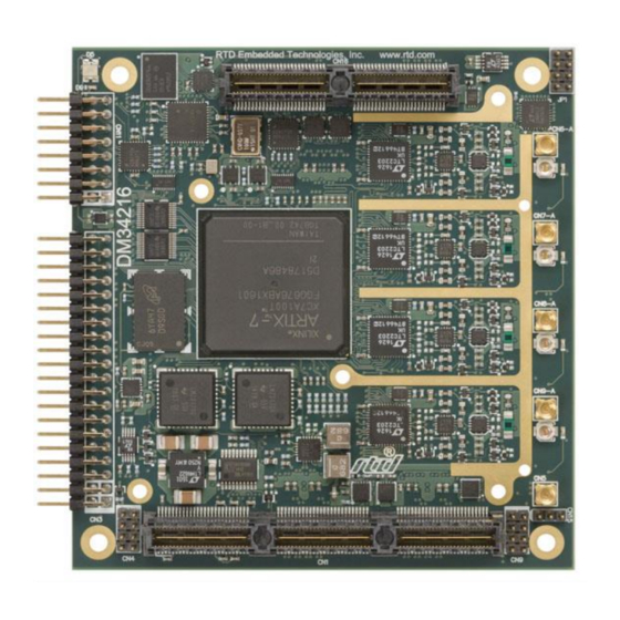
1 Introduction Product Overview The DM34116HR dataModule is a rugged high-speed data acquisition (DAQ) module in the PCIe/104 format which boasts two 16-bit 25 MHz A/D converters and two 16-bit 25Mhz D/A converters. This module provides 2 single-ended analog input channels with software-selectable input ranges and input impedances. -
Page 11: Ordering Information
If you are having problems with your system, please try the steps in the Troubleshooting section of this manual on page 57. For help with this product, or any other product made by RTD, you can contact RTD Embedded Technologies technical support via the following methods: Phone: 1-814-234-8087 Monday through Friday, 8:00am to 5:00pm (EST). -
Page 12: Specifications
2.49996 Max Output Voltage V = DAC + Offset -4.5 +4.5 Resolution Bits Update Rate MSPS Output Impedance Ω External Reference Input Impedance Ω Input Voltage Input Frequency DM34116HR | www.rtd.com User’s Manual RTD Embedded Technologies, Inc. BDM-610010057 Rev A... -
Page 13: Functional Characteristics
In Figure 1, a coherent 250kHz sine wave signal was attached to input Channel 0-3 in the +/-2.5V, 50Ω mode. The FFT was generated using 500000 samples. Figure 1: Gain of 1 FFT | www.rtd.com DM34116HR User’s Manual RTD Embedded Technologies, Inc. BDM-610010057 Rev A... -
Page 14: Figure 2: Gain Of 6 Fft
In Figure 2, a coherent 250kHz sine wave signal was attached to input Channel 0-3 in the +/-0.4167V, 50Ω mode. The FFT was generated using 500000 samples. Figure 2: Gain of 6 FFT | www.rtd.com DM34116HR User’s Manual RTD Embedded Technologies, Inc. BDM-610010057 Rev A... -
Page 15: Board Connection
Handle the board in an antistatic environment and use a grounded workbench for testing and handling of your hardware. Physical Characteristics STEP model is available upon request; contact RTD Tech Support for more information. • Weight: Approximately 99.8 g (0.22 lbs) with heatsink •... -
Page 16: Connectors And Jumpers
PC/104 Specifications on page 58) The DM34116HR is a Type 2 board, and can only connect to either Type 2 PCIe/104 connector. CN16(Top) & CN17(Bottom): Two Bank Connector The Two Bank connector is a high-speed board to board interconnect. Currently the only feature the two bank provides is an independent SyncBus connection. -
Page 17: External I/O Connectors
The SyncBus Connector is a 2 x 8, 0.1” spacing right-angle connector. The pin assignments are shown in Table 6 below. A typical mating connector is a FCI 65043-029LF. Pin 1 is indicated by a square solder pad. DM34116HR | www.rtd.com User’s Manual RTD Embedded Technologies, Inc. BDM-610010057 Rev A... -
Page 18: Jumpers
(GBC_BRD_RST). If this doesn’t fix the issue, the module will need to be power cycled. ADCn Enable LED This LED is green when a ADC channel is enabled. DM34116HR | www.rtd.com User’s Manual RTD Embedded Technologies, Inc. BDM-610010057 Rev A... -
Page 19: Steps For Installing
11. Re-connect the power cord and apply power to the stack. 12. Boot the system and verify that all of the hardware is working properly. Figure 5: Example 104™Stack DM34116HR | www.rtd.com User’s Manual RTD Embedded Technologies, Inc. BDM-610010057 Rev A... -
Page 20: Idan Connections
• Dimensions: 152 mm L x 130 mm W x 24.5 mm H (5.98 in L x 5.12 in W x 0.97 in H) Figure 6: IDAN Dimensions DM34116HR | www.rtd.com User’s Manual RTD Embedded Technologies, Inc. BDM-610010057 Rev A... -
Page 21: Connectors
Digital I/O Connector - 37-pin High Density “D” Female Connector Pin 19 Pin 1 Pin 20 Pin 37 Connector Part #: AMP 1658610-1 Example Mating Connector: TYCO 1658608-1 Table 8: IDAN- DM34116HR 37-Pin High Density "D" Connector DM34116HR Pin # IDAN Pin# Signal DIO0.0 DIO0.2 DIO0.4 DIO0.6 DIO0.8 DIO0.10... -
Page 22: Bus Connectors
The PCIe connector is the connection to the system CPU. The position and pin assignments are compliant with the PCI/104-Express Specification. (See PC/104 Specifications on page 58) The DM34116HR is a Type 2 board, and can only connect to either Type 2 PCIe/104 connector. DM34116HR | www.rtd.com User’s Manual RTD Embedded Technologies, Inc. -
Page 23: Steps For Installing
11. Re-connect the power cord and apply power to the stack. 12. Boot the system and verify that all of the hardware is working properly. Figure 7: Example IDAN System DM34116HR | www.rtd.com User’s Manual RTD Embedded Technologies, Inc. BDM-610010057 Rev A... -
Page 24: Functional Description
Functional Description Block Diagram The Figure below shows the functional block diagram of the DM34116HR. The various parts of the block diagram are discussed in the following sections. Gain PCIe x4 Channel 0 Impendence Input control Offset Gain Channel 1... -
Page 25: Programmable Clock
5.4.1 LOCK ENERATOR The DM34116HR provides a method to synchronize the clock generator on multiple DM34116HR modules using the syncbus. This allows the ADC on multiple modules to be synchronize within one System Clock cycle. This process should be performed once all ADC frequencies have been set. -
Page 26: Capture Window
FIFO for DMA. Each sample is packed into 32-bits. Advanced Interrupts The DM34116HR has an advanced interrupt block that can generate an interrupt on a match, event or strobe. The interrupts are across all 32-digital input of the function block. The bits can be individually selected. -
Page 27: Quad Pulse Width Modulator
IDTH ODULATOR The DM34116HR features a quad PWM output functional block with DMA. The PWM is available with the output pin peripherals are configured as PWM. All the PWM outputs have the same period. The pulse width of each of the four outputs is individually adjustable. -
Page 28: External Clocking
XTERNAL LOCKING The DM34116HR features an external clocking function block. This feature allows the user to input a clock to drive a CLK_BUSn signal or output a CLK_BUSn signal. The CLK_SRCn are used to drive the CLK_BUSn signal which are part of the most FPGA function blocks. -
Page 29: Temperature Sensor
Each ADC converter supports a 1023 sample FIFO for DMA. Each sample packed into a 32-bit word. Full-Scale Input Range The DM34116HR has a programmable gain input per channel. This gain can be programed for 0.5, 0.75, 1, 1.5, 2, 3, 4, 6 to achieve input ranges ±5V, ±3.3V, ±2.5V, ±1.667V, ±1.25V, ±0.833V, ±0.625V, ±0.416V. -
Page 30: Initializing The Adc Converter
IMPLIFIED BLOCK DIAGRAM OF ANALOG INPUT The following figure shows the front end circuit for the DM34116HR. It also shows the names of the FPGA registers in bold and the different ways the front-end can be configured for different modes of operation. -
Page 31: Input Connection Examples
[GAIN_05] = 0 Analog OpAmp Input CHn_Front_End_Config [IMPED] = 0 To Diff Gain Control Diff Amp 2.5V CHn_Front_End_Config [GAIN] = 0 OpAmp -2.5V Figure 11:High Impedance Bipolar Example DM34116HR | www.rtd.com User’s Manual RTD Embedded Technologies, Inc. BDM-610010057 Rev A... -
Page 32: Analog Output
DAC Output Range The DM34116HR DAC output has range of ±2.5V. However, the module features an additional DAC that allows you to adjust the offset of high speed DAC output. The min/max voltage out of the output buffer is ±4.5V. -
Page 33: Figure 13: Output Circuit
5.9.2 IMPLIFIED BLOCK DIAGRAM OF ANALOG OUTPUT The following figure shows the output circuit for the DM34116HR. It also shows the names of the FPGA registers in bold and how the output can be configured. 16bit 25MHz D/A Front_End_Config [Output_Enable]... -
Page 34: Table 11: Function Block Mapping
‘0’. This is typically used for interrupt status registers. • Read Only: This register can only be read. NOTE: Writing to Read-Only registers may have unexpected results. Function Block Mapping Below is the Function Block slot mapping for the DM34116HR. Table 11: Function Block Mapping Slot Description Connector... -
Page 35: Table 12: Base Functional Block
Write a value of 0xAA to this register to reset the board. 6.1.4 GBC_PDP (R This register contains the PDP number for this board in decimal. 6.1.5 GBC_BUILD (R Unique 32-bit build number for every FPGA build. DM34116HR | www.rtd.com User’s Manual RTD Embedded Technologies, Inc. BDM-610010057 Rev A... - Page 36 _DMA (R FFSET This is the offset from the beginning of the Functional Block section (typically the offset in BAR2) that the Functional Block DMA Registers resides in. DM34116HR | www.rtd.com User’s Manual RTD Embedded Technologies, Inc. BDM-610010057 Rev A...
-
Page 37: Table 13: Dma Registers
Used_Desc bit (below) if the next buffer has the Used bit set. However, it will not generate an interrupt, and will not PAUSE the DMA engine. Examples are continuous output from a DAC, or very large Pre-trigger buffering using system memory. DM34116HR | www.rtd.com User’s Manual RTD Embedded Technologies, Inc. BDM-610010057 Rev A... - Page 38 This is the size in bytes of the buffer for DMA Channel m, buffer n. It must be an integer number of double-words (i.e. b[1:0] are reserved). The actual size is FB_DMAm_SIZEn + 4 Bytes. The maximum buffer size is 16MB. DM34116HR | www.rtd.com User’s Manual RTD Embedded Technologies, Inc. BDM-610010057 Rev A...
-
Page 39: Table 14: Functional Block Header
NOTE: This register is not implemented on every function block. You must check each function block’s register map to see if this register is defined. DM34116HR | www.rtd.com User’s Manual RTD Embedded Technologies, Inc. BDM-610010057 Rev A... -
Page 40: Table 15: High Speed A/D Functional Block
BAR2: Analog to Digital Converter (ADC) This Function Block is for the Analog to Digital converter. The DM34116HR has two ADC Function blocks, one for each of the ADC inputs. The ADC0 input is associated with the lower-numbered ADC Function Block, and ADC1 is associated with the higher-numbered ADC Function Block. - Page 41 ������������ ���������� ������������������ = (2 × ������_������) Maximum clock rate is 25Mhz, CLK_DIV = 0x04 Minimum clock rate is 1Mhz, CLK_DIV = 0x64 Disabling clock, CLK_DIV = 0x00 DM34116HR | www.rtd.com User’s Manual RTD Embedded Technologies, Inc. BDM-610010057 Rev A...
- Page 42 B4: Stop Trigger B5: Post-Stop Buffer Filled B6: Sampling has completed, and the FIFO is empty (all data transferred to host) B7: Pacer – The pacer clock has ticked. DM34116HR | www.rtd.com User’s Manual RTD Embedded Technologies, Inc. BDM-610010057 Rev A...
- Page 43 B[0]:Shutdown 0 = ADC is enabled 1 = ADC is disabled 6.4.18 FIFO_DATA_CNT (R This register shows the current sample count that is available in the ADC’s FIFO. DM34116HR | www.rtd.com User’s Manual RTD Embedded Technologies, Inc. BDM-610010057 Rev A...
-
Page 44: Figure 14: Filter Response With Each Order Value
Reading a value of ‘0’ indicates that the event has not occurred. Writing a ‘1’ will clear that bit. B0: ‘1’ = Low Threshold has been crossed B1: ‘1’ = High Threshold has been crossed DM34116HR | www.rtd.com User’s Manual RTD Embedded Technologies, Inc. BDM-610010057 Rev A... - Page 45 This register provides direct access to the DMA FIFO. It can be used to access the data without the use of the DMA engine. The DMA engine for this channel must be set to “Pause.” Each register access advances to the next sample. DM34116HR | www.rtd.com User’s Manual RTD Embedded Technologies, Inc. BDM-610010057 Rev A...
-
Page 46: Table 16: High Speed D/A Functional Block
BAR2: Digital to Analog Converter (DAC) This Function Block is for the Digital to Analog converter. The DM34116HR has two DAC Function blocks, one for each of the DAC outputs. The DAC0 input is associated with the lower-numbered DAC Function Block, and DAC1 is associated with the higher-numbered DAC Function Block. - Page 47 ������������ ���������� ������������������ = (2 × ������_������) Maximum clock rate is 25Mhz, CLK_DIV = 0x04 Minimum clock rate is 1Mhz, CLK_DIV = 0x64 Disabling clock, CLK_DIV = 0x00 DM34116HR | www.rtd.com User’s Manual RTD Embedded Technologies, Inc. BDM-610010057 Rev A...
- Page 48 B1: Channel Marker – One of the channels has an enabled marker. B2: Reserved B3: Start Trigger B4: Stop Trigger B5: Post-Stop Conversions Completed B6: Reserved B7: Reserved DM34116HR | www.rtd.com User’s Manual RTD Embedded Technologies, Inc. BDM-610010057 Rev A...
- Page 49 This register provides configuration to the Front End for the DAC. B[0]: Output_Enable 0 = Disable 1 = Enable B[1]: Reserved DM34116HR | www.rtd.com User’s Manual RTD Embedded Technologies, Inc. BDM-610010057 Rev A...
- Page 50 This register provides direct access to the DMA FIFO. It can be used to access the data without the use of the DMA engine. The DMA engine for this channel must be set to “Pause.” Each register access advances to the next conversion. DM34116HR | www.rtd.com User’s Manual RTD Embedded Technologies, Inc. BDM-610010057 Rev A...
-
Page 51: Table 17: Advance Dio Functional Block
0x04: Uninitialized. This is the power-on state. No converter initialization has taken place. Sampling is stopped, and all counters are reset and the triggering state machine is reset. DM34116HR | www.rtd.com User’s Manual RTD Embedded Technologies, Inc. BDM-610010057 Rev A... - Page 52 6.6.5 STOP_TRIG (R RITE Selects the stop trigger from the clock bus. Refer to CLK_SRC section above, for list of valid values. DM34116HR | www.rtd.com User’s Manual RTD Embedded Technologies, Inc. BDM-610010057 Rev A...
- Page 53 A function block can drive multiple different Clock Buses. However, a Clock Bus N should not be driven by more than one function block at the same time or the clock signal will be undefined. DM34116HR | www.rtd.com User’s Manual RTD Embedded Technologies, Inc. BDM-610010057 Rev A...
- Page 54 The Capture register latches the input ports when an interrupt is generated. All values are latched, regardless of the ADV_INT_MASK register, or DIO_DIRECTION. This register can be written to when ADV_INT_MODE is set to Disabled. DM34116HR | www.rtd.com User’s Manual RTD Embedded Technologies, Inc. BDM-610010057 Rev A...
- Page 55 This register shows the current sample count in Digital I/O channel FIFO. 6.6.21 CH _MAX_FIFO_SIZE (R This register shows the max number of samples that the Digital I/O channel FIFO can hold. DM34116HR | www.rtd.com User’s Manual RTD Embedded Technologies, Inc. BDM-610010057 Rev A...
- Page 56 This register provides direct access to the DMA FIFO. It can be used to access the data without the use of the DMA engine. The DMA engine for this channel must be set to “Pause.” Each register access advances to the next sample. DM34116HR | www.rtd.com User’s Manual RTD Embedded Technologies, Inc. BDM-610010057 Rev A...
-
Page 57: Table 18:Pwm Functional Block
0x03: Go, Re-arm. After filling the buffer with the Post-Stop samples and the FIFO is empty, the triggering state machine is restarted, i.e. FIFO is filled with Pre-Start samples and waits for a start trigger. DM34116HR | www.rtd.com User’s Manual RTD Embedded Technologies, Inc. BDM-610010057 Rev A... - Page 58 The current value of the Clock Divide Counter. This counter starts at a value of CLK_DIV, and counts down. When it reaches zero, a sample is taken. This is useful when using a slow sample clock. DM34116HR | www.rtd.com User’s Manual RTD Embedded Technologies, Inc. BDM-610010057 Rev A...
- Page 59 This register shows the current sample count that is available in the interval counter FIFO. 6.1.13 CH _MAX_FIFO_SIZE (R This register shows the max number of samples that the interval counter FIFO can hold. DM34116HR | www.rtd.com User’s Manual RTD Embedded Technologies, Inc. BDM-610010057 Rev A...
- Page 60 This register provides direct access to the DMA FIFO. It can be used to access the data without the use of the DMA engine. The DMA engine for this channel must be set to “Pause.” Each register access advances to the next sample. DM34116HR | www.rtd.com User’s Manual RTD Embedded Technologies, Inc. BDM-610010057 Rev A...
-
Page 61: Table 19: Incremental Encoder Functional Block
0x03: Go, Re-arm. After filling the buffer with the Post-Stop samples and the FIFO is empty, the triggering state machine is restarted, i.e. FIFO is filled with Pre-Start samples and waits for a start trigger. DM34116HR | www.rtd.com User’s Manual RTD Embedded Technologies, Inc. BDM-610010057 Rev A... - Page 62 The current value of the Clock Divide Counter. This counter starts at a value of CLK_DIV, and counts down. When it reaches zero, a sample is taken. This is useful when using a slow sample clock. DM34116HR | www.rtd.com User’s Manual RTD Embedded Technologies, Inc. BDM-610010057 Rev A...
- Page 63 0x88: Positive rollover - Indicates channel has transitioned from 0xFFFFFFFF to 0x00000000. o 0x89: Negative rollover - Indicates channel has transitioned from 0x00000000 to 0xFFFFFFFF. o 0x8A: High threshold crossed. o 0x8B: Low threshold crossed. DM34116HR | www.rtd.com User’s Manual RTD Embedded Technologies, Inc. BDM-610010057 Rev A...
- Page 64 This register provides direct access to the DMA FIFO. It can be used to access the data without the use of the DMA engine. The DMA engine for this channel must be set to “Pause.” Each register access advances to the next sample. DM34116HR | www.rtd.com User’s Manual RTD Embedded Technologies, Inc. BDM-610010057 Rev A...
-
Page 65: Table 20:External Clocking Functional Block
Signal EXT_CLK_GATE7 EXT_CLK_GATE6 EXT_CLK_GATE5 EXT_CLK_GATE4 EXT_CLK_GATE3 EXT_CLK_GATE2 6.3.4 EXT_CLK_DIR (R RITE Selects the direction of the External Clocking bits. 0=input, 1=output. All pins default to inputs at power-up. DM34116HR | www.rtd.com User’s Manual RTD Embedded Technologies, Inc. BDM-610010057 Rev A... - Page 66 0x82: Clock Gated (Low): CLK_BUSn will be inputted when the EXT_CLK_GATEn corresponding gate value is low, this doesn’t affect when outputting a clock. DM34116HR | www.rtd.com User’s Manual RTD Embedded Technologies, Inc. BDM-610010057 Rev A...
-
Page 67: Table 21: Temperature Sensor Functional Block
Selects the 10MHz reference clock that is used to generate the system and ADC clocks. B[3:0]: o 0x00: Onboard Reference Clock o 0x01: External Reference Clock (CN5) o 0x02: SyncBus Reference Clock, (SyncBus3 of CN11) o 0x03: Reserved DM34116HR | www.rtd.com User’s Manual RTD Embedded Technologies, Inc. BDM-610010057 Rev A... - Page 68 B0: for reads, 0 = Busy, 1 = Synchronization is ready. Write 0x01 to start the synchronization process. DM34116HR | www.rtd.com User’s Manual RTD Embedded Technologies, Inc. BDM-610010057 Rev A...
-
Page 69: Table 23: Capture Window Functional Block
0x03: Go, Re-arm. After filling the buffer with the Post-Stop samples and the FIFO is empty, the triggering state machine is restarted, i.e. FIFO is filled with Pre-Start samples and waits for a start trigger. DM34116HR | www.rtd.com User’s Manual RTD Embedded Technologies, Inc. BDM-610010057 Rev A... - Page 70 Each bit corresponds to an interrupt source. A value of ‘1’ enables the source, and a value of ‘0’ disables it. See below for a description of the sources. DM34116HR | www.rtd.com User’s Manual RTD Embedded Technologies, Inc. BDM-610010057 Rev A...
- Page 71 0x80: Capture Window – Indicates state of window, high when during capture and low when during delay o 0x81: Reserved o 0x82: Reserved o 0x83: Start Trigger o 0x84: Reserved o 0x85: Reserved o 0x86: Reserved DM34116HR | www.rtd.com User’s Manual RTD Embedded Technologies, Inc. BDM-610010057 Rev A...
- Page 72 Sets the width of delay counter n. Delay Counter = (DELAY_COUNTER_n) / (Pacer Clock). 6.6.13 CAPTURE_COUNTER_ RITE Sets the width of capture counter n. Capture Counter = (CAPTURE_COUNTER_n) / (Pacer Clock). DM34116HR | www.rtd.com User’s Manual RTD Embedded Technologies, Inc. BDM-610010057 Rev A...
-
Page 73: Table 24: Syncbus Functional Block
SyncBus will not receive or transmit. This bit must be enabled in order to use the SyncBus. B0: Enable SyncBus driver, 0 = disabled (low power), 1 = enabled. DM34116HR | www.rtd.com User’s Manual RTD Embedded Technologies, Inc. BDM-610010057 Rev A... - Page 74 PLL_SYNC (R RITE This register is used to issue a PLL sync signal across multiple DM34116HR. When enabling the pll sync mode, SYNCBUS_0 is repurposed to send/receive the pll sync signal. Refer to section xxx for more information. B0: SYNC_Enable, 0 = disabled (Normal SyncBus Operation), 1 = Allows Clock Synchronization B3: Go/Busy(Sticky Register) When this bit is high (‘1’) it is ready to synchronize the boards.
- Page 75 B[1]: Data be to driven on SYNC1p/n when the SyncBus is configured for GPIO mode and SYNC_OUT_EN is set. • B[0]: Data be to driven on SYNC0p/n when the SyncBus is configured for GPIO mode and SYNC_OUT_EN is set. DM34116HR | www.rtd.com User’s Manual RTD Embedded Technologies, Inc. BDM-610010057 Rev A...
-
Page 76: Table 25: Programmable Clock Functional Block
0x03: Go, Re-arm. After filling the buffer with the Post-Stop samples and the FIFO is empty, the triggering state machine is restarted, i.e. FIFO is filled with Pre-Start samples and waits for a start trigger. DM34116HR | www.rtd.com User’s Manual RTD Embedded Technologies, Inc. BDM-610010057 Rev A... - Page 77 The current value of the Clock Divide Counter. This counter starts at a value of CLK_DIV, and counts down. When it reaches zero, a sample is taken. This is useful when using a slow sample clock. DM34116HR | www.rtd.com User’s Manual RTD Embedded Technologies, Inc. BDM-610010057 Rev A...
- Page 78 ’0’ = Interval Counter is disabled ’1’ = Interval Counter is enabled 6.8.13 CH _FIFO_DATA_CNT (R This register shows the current sample count that is available in the interval counter FIFO. DM34116HR | www.rtd.com User’s Manual RTD Embedded Technologies, Inc. BDM-610010057 Rev A...
- Page 79 This register provides direct access to the DMA FIFO. It can be used to access the data without the use of the DMA engine. The DMA engine for this channel must be set to “Pause.” Each register access advances to the next sample. DM34116HR | www.rtd.com User’s Manual RTD Embedded Technologies, Inc. BDM-610010057 Rev A...
- Page 80 If problems persist, or you have questions about configuring this product, contact RTD Embedded Technologies via the following methods: Phone: +1-814-234-8087 E-Mail: techsupport@rtd.com Be sure to check the RTD web site (http://www.rtd.com) frequently for product updates, including newer versions of the board manual and application software. DM34116HR | www.rtd.com User’s Manual RTD Embedded Technologies, Inc.
- Page 81 PCI and PCI Express Specification A copy of the latest PCI and PCI Express specifications can be found on the webpage for the PCI Special Interest Group: www.pcisig.com DM34116HR | www.rtd.com User’s Manual RTD Embedded Technologies, Inc. BDM-610010057 Rev A...
- Page 82 RTD Embedded Technologies, Inc. warrants the hardware and software products it manufactures and produces to be free from defects in materials and workmanship for one year following the date of shipment from RTD Embedded Technologies, Inc. This warranty is limited to the original purchaser of product and is not transferable.
- Page 83 RTD Embedded Technologies, Inc. 103 Innovation Boulevard State College, PA 16803 USA Telephone: 814-234-8087 Fax: 814-234-5218 www.rtd.com sales@rtd.com techsupport@rtd.com Copyright 2019 by RTD Embedded Technologies, Inc. All rights reserved.
Need help?
Do you have a question about the DM34116HR and is the answer not in the manual?
Questions and answers