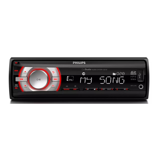
Table of Contents
Advertisement
Quick Links
DISMANTLING INSTRUCTIONS.................................................2
BLOCK DIAGRAM........................................................................3
WIRING DIAGRAM......................................................................4
CIRCUIT DIAGRAM MAIN BOARD.............................................5-6
CIRCUIT DIAGRAM PANEL BOARD.........................................7
2012-4-26
MAIN PCB COMPONENT LAYOUT............................................8-9
PANEL PCB COMPONENT LAYOUT.........................................10-11
SET EXPLODER VIEW DRAWING................................................12
TROUBLE SHOOTING...................................................................13-14
CE132/all ,--G,R/all
Advertisement
Table of Contents

Summary of Contents for Philips CE132/all
-
Page 1: Table Of Contents
CE132/all ,--G,R/all DISMANTLING INSTRUCTIONS..........2 MAIN PCB COMPONENT LAYOUT..........8-9 BLOCK DIAGRAM................3 PANEL PCB COMPONENT LAYOUT.........10-11 WIRING DIAGRAM..............4 SET EXPLODER VIEW DRAWING..........12 CIRCUIT DIAGRAM MAIN BOARD..........5-6 CIRCUIT DIAGRAM PANEL BOARD.........7 TROUBLE SHOOTING..............13-14 2012-4-26... -
Page 2: Dismantling Instructions
The procedure of disassembling the unit Remove A, B screws in the back cover as below picture showed; Use tweezer to prize up top cover as the blue arrow direction which showed as below picture and remove the top cover 2.) Remove the four screws in C,D,E,F position in the heat sink, then remove the G screw in left side of the unit and the H, I screws which were for fixing the main board;... -
Page 4: Wiring Diagram
Wiring Diagram... -
Page 5: Circuit Diagram Main Board
CIRCUIT DIAGRAM -MAIN BOARD... -
Page 7: Circuit Diagram Panel Board
CIRCUIT DIAGRAM -PANEL BOARD LED 901 BT: NO BT: 180R R911 220R R912 330R R913 470R R914 680R R915 R916 R918 R919 180R R921 220R R922 330R R923 680R R925 R926 470R R924... -
Page 8: Main Pcb Component Layout
PCB LAYOUT-MAIN BOARD TOP SIDE VIEW... - Page 9 PCB LAYOUT-MAIN BOARD BOTTOM SIDE VIEW...
-
Page 10: Panel Pcb Component Layout
PCB LAYOUT-PANEL BOARD TOP SIDE VIEW... - Page 11 PCB LAYOUT-PANEL BOARD BOTTOM SIDE VIEW...
-
Page 12: Set Exploder View Drawing
SET EXPLODER VIEW DRAWING... -
Page 13: Trouble Shooting
CE132 2012-4-10 Product Model Date failure failure cause remark phenomena a. To check whether the CN1(ISO) connector of the tail of the unit is connect well , Whether it is loose of the 15A fuse of the ISO, or insert non in place. b. - Page 14 failure failure cause remark phenomena a. To check whether the USB/SD signal format is correspond to the request of the unit. b. To check the voltage of the the uppermost pin of the USB connector, should be +5V0. USB defective c.


Need help?
Do you have a question about the CE132/all and is the answer not in the manual?
Questions and answers