Advertisement
Quick Links
Advertisement

Related Manuals for KANDA STK300


Summary of Contents for KANDA STK300
- Page 1 STK300 U ANUAL Published by ANDA YSTEMS www.kanda.com Page...
- Page 2 Kanda Systems Ltd. without notice due to product improvements or other reasons. Kanda Systems Ltd. assumes no liability for the accuracy or use of the information. Kanda Systems Ltd. assumes no responsibility for any damage, or infringement of any third-party’s rights, originating in the use of any product data, diagrams, charts or...
- Page 3 AVRMEGA603L Upgrades for new devices will be available via the Internet from www.kanda.com Kanda Systems cannot be held responsible for any errors or omissions in this system. The limit of any liabilities is limited to providing replacement hardware or software.
- Page 4 Getting Started Unpacking the system You will find the following items in the box: • Main Board • 1 Disk set • ISP Dongle • ISP Ribbon Cable System Requirements The minimum hardware and software requirements are: • 80386 processor or above (486 or above recommended) •...
- Page 5 Connecting the system Connect Lead supplied to Dongle and insert in PC Printer Port or Serial Port Power Supply 9 - 15 V DC 7 - 12V AC Plug header on Power Connector lead into 5.5/2.1 Barrel Programming Interface - Key way gives orientation Programming RS232...
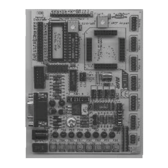
- Page 6 Hardware Description The main features of the board are shown in the diagram below. Analog Reference LK1 - Cut for A/D Voltage Adjustment LCD Connector External Reference Contrast Adjustment Analog I/P External Memory Plug in MEGA Expansion board here Ext. SRAM Port A Digital Address Latch IC for RAM...
- Page 7 Jumpers and links and their functions Jumper Function Open Closed Default Voltage select 3.3V Open Brown out select 2.9V 4.5V Closed RS232 RXD Port E.0 Port E.0 RS232 TXD Port E.1 Port E.1 Port B LEDs LEDs Disabled LEDs Enabled Closed Port D Switches...
- Page 8 Note: If you have any problems installing the software or suspect that you have faulty media please contact our technical support department. Please make sure you have the latest version of the software installed before contacting the support line. Telephone: +44 (0) 1970 621041 Fax: +44 (0) 1970 621040 support@kanda.com E-mail: Website www.kanda.com Page...
-
Page 9: How To Use The Software
How to use the Software The Programmer software is shown below: Window Main Menu Hardware Selection Device Security Selection Selection Settings Status Indictor and ASCII Pane Message Line Memory Buffer - Editable Window Red = Error - Editable Yellow = In Progress Green = OK Overview The programmer uses three main displays:... - Page 10 Configuring the software 1. The first step is to choose the type of hardware connection, using the drop-down list at the top right of the screen. Select E-ISP Serial Port or E-ISP Parallel Port as required. Ensure that the board is connected to the serial or parallel port as appropriate. 2.
- Page 11 Yellow Operation is taking place This light coding applies for all operations. 3. When a file has been loaded into the Flash memory and the EEPROM memory if required, the programmer is ready for programming operations. EEPROM data (or Flash data) can be typed directly into the buffer windows instead of being loaded from a file.
- Page 12 Check the required functions. All the selected functions will run when Auto-Program (F5) is used. If Program Fuses is available and checked, then another dialog box will appear after this list is closed where you can set device specific fuses. Note: Erase the device before programming unless you are adding extra data to existing data in the device.
- Page 13 Menu and Option Descriptions File Menu Load Select memory area/buffer window to load (Flash or EEPROM), then open the Intel Hex file in the Open File dialog box. A red status warning light indicates that the file load was unsuccessful. This may be because the file is not Intel Hex or it is too large for the selected buffer/memory.
- Page 14 Other Controls Device Selector Located at the top left of the screen, this drop-down list is used to select the required device. Make sure that this selection matches the device you have plugged into the board. Obtain an upgrade to support new devices as they are released. Security Located in the center of the screen, Security is used to select type of access to the device once it has been programmed.
- Page 15 • Status This window lists all the operations, status and error messages that have occurred during the current session. To clear the messages displayed, right-click and select Clear Status. Status Indicator Displays a visual result of the current operation - Red means that the operation failed, Yellow means it is in progress and Green means it was successful.
- Page 16 Programming Using the Board Device Orientation Before programming a device using the programming module, the device adapter must be inserted correctly into the programming unit. The adapter itself has a corner cut off, which locates pin 1 of the device and matches the marking on the main unit. This adapter should be pre-fitted, but can be replaced if the device programming life is exceeded - refer to your supplier to obtain new device adapter.
- Page 17 Brown Out Detector The brown out detector circuit is used to detect voltage drops. If a short glitch occurs in the power, this circuit ensures that the processor resets properly rather than operating randomly. The brown out detector must be set to the same voltage as the circuit voltage (Vcc) - 3.3V or 5V. For 3.3V operation, jumper JP2 must be removed (jumper open) and for 5V operation it must be closed.
- Page 18 Board Applications Using Switches and LEDs The LEDs are connected through a 1K resistor network to Port B. The switches are connected to Port D. The switches and LEDs can be disconnected if required, so to use them, ensure that the jumpers labeled Port B and Port D are closed.
- Page 19 The last header labeled Misc has connections to processor pins other than the port pins. Cut out marked on board to give orientation Read EXTERNAL Write RESET Extra Connection for Extra Connection for Ground If external operations do not want pull-ups on the port pin, both the switches and the LEDs can be disconnected from the processor.
- Page 20 Using Internal Reference To use the internal (on-board) Voltage Reference, the pot marked AREF is used to set the voltage level. The voltage level can be measured with a meter connected to the header pins labeled Analog Ref and Analog Gnd in the above diagram or from the two holes marked Meter (+ and -). Using External Reference To use the A2D converters with an external Voltage Reference, the link marked LK1 must be cut.
- Page 21 RAM Socket pin layout I/O7 I/O0 I/O6 I/O1 I/O5 I/O2 I/O4 I/O3 Address Latch. The board connections are for a 74HC573 device. This device will operate reliably with the 4 MHz crystal supplied but if a faster crystal is inserted, a faster version of this device may be required - 74AHC573 or 74FHC573.
- Page 22 Using LCD Connections The header marked LCD interface is for a standard 2 X 16 LCD. The connections are shown on the board and in the following table. Connection Function Name Ground 0V Vcc - must be 5V Contrast Register Select- A14 Not Write Enable Data Bit 0...
- Page 23 Programming In System Devices can be programmed in your circuit rather than on the board. For In System Programming, (ISP), the 10 way programming lead is connected to a dual row 10 way (0.1" pitch) header on your circuit. You will need to use either a multiplexer chip (such as a 4053) or wire directly to the Pins of the device.
- Page 24 Interface using resistors Programming Header MISO is called PDO and MOSI is PDI on Mega devices MISO - Port E bits 0 and 1 NOT pins on Port B. MOSI SCK-PB1 User Circuit PDO-PE1 PDI-PE0 Reset Typical resistor values would be 1K. This circuit is fine if ports PB7, PE0 and PE1 are used as inputs in your circuit and no communications are required.
- Page 25 The multiplexer select can be driven from the LED connection on the programming lead (as can a low power LED with its cathode connected to the LED connection via a suitable resistor -1K5 is fine-). If you use this connection then the output will be low (0) during programming and a 1 at all other times.
- Page 26 Application Builder Application Builder Speed Button This image indicates which icon to select, i.e. the one on the left. Alternatively, use the File Menu and select Application Builder. Start Window The first step is to select the device you want to use from the list on the top left, labelled Devices. Watchdog Timer Page...
- Page 27 The on-board Watchdog Timer (WDT) can be enabled or disabled. If it is enabled a prescaler can be applied to lengthen the WDT time-out period. The minimum time-out period is 16 mS and the maximum is 2048 mS. If emulation is required it is recommended that the WDT is disabled. SRAM External SRAM can be used with some AVR devices - see device data sheets for details.
- Page 28 Peripherals Window Peripherals The various peripherals are enabled or disabled depending on which device is selected, so this list acts as a map of the peripherals available on each device. Each peripheral has a separate page in the Application Builder. Ports The ports required are selected in this section.
- Page 29 Sleep and Power Down Window XTAL The oscillator frequency can be divided by a factor between 1 and 129 to reduce power consumption when processing power requirements are low. Set the divide factor required in the spin box. Checking the XTAL Divide box will enable XTAL Divide immediately, but in most applications this will not be required, so leave the box unchecked and set the XTALEN bit in the XDIV register when needed (XDIV.7).
- Page 30 TOSC2 pins (pins 19 and 18). It is optimized for a 32.768 KHz crystal for use as a Real Time Clock, and this crystal is fitted on the STK300 board. Timer 0 can also operate in PWM Mode or Output Compare Mode or neither.
- Page 31 Non-inverted - Cleared on upcount, set on downcount Inverted - Set on upcount, cleared on downcount Output Compare The value of Timer 0 is compared with the value set in the Compare Value Field. When a match is detected, the effect on the output pin (OC0 - pin 14) is set by the Output radio buttons. If the Clear Timer box is checked, the timer is reset to $00 in the CPU clock cycle after a match.
- Page 32 Input Capture This option is also always available. When the Edge selected (rising or falling edge) is detected on ICP pin, the current value of Timer 1 is copied to the Input Capture Register - ICR1. The Input Capture flag is also set and an interrupt can be generated - Timer 1 Capture. The other two options are PWM Mode and Output Compare Mode and these are mutually exclusive.
- Page 33 Timer 2 Window Timer 2 is an 8-bit Timer/Counter. Standard Operation Page...
- Page 34 Regardless of which other options are selected, Timer 2 can operate in Timer or Counter mode If Source is set to Timer, Timer 2 increments from the system clock. If it is set to Counter, it increments on either rising or falling edge (set by Edge) on T2 pin (pin32 - PD7). A prescaler can be applied to increase overflow time in timer mode.
- Page 35 External Interrupts Window The AVRMEGA has 23 interrupt sources, including 8 external interrupts (INT0..INT7). If this page or the next page (Interrupts) are selected, an interrupt template will be generated even if no actual interrupts are checked. Interrupts INT0 to INT3 are always low leveled triggered on pin 25 to pin 28 (PD0..PD3). To select an interrupt, check its box.
- Page 36 Interrupts Window To enable an interrupt, check the corresponding checkbox- note that the external interrupts are on a separate page. An interrupt template is generated even if no individual interrupts are checked. The Comparator section is enabled if the Analogue Comparator Interrupt is checked. The comparator can be disabled, and the cause of the interrupt can be selected.
- Page 37 UART and SPI Port Window UART The Use UART checkbox can be cleared if SPI is required and UART is not needed. Crystal Frequency is a drop down box containing the frequency of the crystal currently on your circuit. The baud rate is that of the COM port being used to communicate with the device. Assistance with this can be found within your operating system’s documentation.
- Page 38 Analog to Digital Converter Window ADC Enable starts the ADC. Please read the ATMEL data book for information on the dummy conversion needed. ADC Free Run Makes the ADC constantly convert, continuously updating the ADC Data Register. If this box is not checked, the ADC operates in Single Conversion Mode and the ADSC bit (ADCSR.6) must be set every time a conversion is required..
- Page 39 ADC Prescaler Slows the converter’s input clock down when dealing with XTAL frequencies above 100kHz. The maximum clock frequency for the ADC is 200KHz (50KHz to 200KHz) so the main oscillator must be prescaled appropriately. ADC Channels Used Selects which input lines (AD7..AD0)are to be used in multiplexed ADC operations. Any pins not used can be used for standard digital inputs - Port F.
- Page 40 Standard Ports Windows This page is representative of the set-up values for the different standard I/O Ports (A, B, D and E). The left-hand column controls whether the port data line is an input (checked) or an output (clear). The second column controls whether the internal pull-up is enabled (checked) or disabled (clear) - inputs only.
- Page 41 Port C Window Port C is output only, so the only choice is initial output value. If external SRAM is enabled, then this port is used for the upper byte of the address and is therefore disabled. Page...
- Page 42 Port F Window Port F is input only. Any bits not used by the ADC can be used for standard input. Page...
- Page 43 Technical Support About Kanda Systems We, at Kanda Systems, design and manufacture all of our own products in the Principality of Wales. We can also undertake custom design work with both Software (high and low level) and hardware designs. Please contact us if you would like help with any projects.
- Page 44 It has been passed for conductivity and radiation and conforms to the regulations in all respects. However, neither Kanda Systems or Atmel can be held accountable for any user supplied equipment, such as Power supplies and computers, used with this system. If these parts do not conform to the EMC regulations, then the complete system will not conform to standards.
- Page 45 Page...
Need help?
Do you have a question about the STK300 and is the answer not in the manual?
Questions and answers