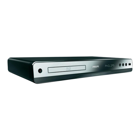
Philips BDP5180 Service Manual
Blu-ray disc player
Hide thumbs
Also See for BDP5180:
- Brochure (3 pages) ,
- User manual (52 pages) ,
- Quick start manual (2 pages)
Advertisement
Quick Links
Blu-ray Disc Player
©
Copyright 2010 Philips Consumer Electronics B.V. Eindhoven, The Netherlands
All rights reserved. No part of this publication may be reproduced, stored in a retrieval system or
transmitted, in any form or by any means, electronic, mechanical, photocopying, or otherwise without
the prior permission of Philips.
Published by SL 1052 Service Audio Printed in The Netherlands Subject to modification
Version 1.1
Version 0.0
TABLE OF CONTENTS
Location of PCB Boards..................................................1-1
Technical Specifi cations ....................................................... 1-2
Safety Instruction, Warning & Notes ..................................... 1-3
Mechanical and Dismantling Instructions ................................2
Software Version & Upgrades, Region Code Change .............3
Trouble Shooting Chart ...........................................................4
Set Wiring Diagram .................................................................5
Electrical Diagrams and PCB layouts ......................................6
Set Mechanical Exploded view & Parts List ............................7
Revision List ............................................................................8
BDP5180/12/51
Page
CLASS 1
LASER PRODUCT
©
314178535600
B
GB
GB
Advertisement

Related Manuals for Philips BDP5180


Summary of Contents for Philips BDP5180
-
Page 1: Table Of Contents
LASER PRODUCT © Copyright 2010 Philips Consumer Electronics B.V. Eindhoven, The Netherlands All rights reserved. No part of this publication may be reproduced, stored in a retrieval system or transmitted, in any form or by any means, electronic, mechanical, photocopying, or otherwise without the prior permission of Philips. -
Page 2: Location Of Pcb Boards
LOCATION OF PCB BOARDS: MAIN BD POWER BD LOADER FRONT BD SWITCH BD FRONT CABINET VERSION VARIATIONS Type /Versions: BDP5180 Service policy Board in used: MAIN BOARD POWER BOARD FRONT BOARD FRONT CABINET LOADER LOADER SWITCH SWITCH BOARD * TIPS : C -- Component Lever Repair. -
Page 3: Technical Specifications
• Specifications are indicative (subject to change). Technical Specifications For on-line product support please use the following website: http://www.p4c.philips.com/cgi-bin/dcbint/cpproduct_selector.pl Here is product information available, as well as getting started, user manuals, frequently asked questions and software & drivers. Directions for Use You can download this information from the following websites: http://www.philips.com/support... - Page 4 Make sure that, • Use only lead-free soldering tin Philips SAC305 with order during repair, you are connected with the same potential as code 0622 149 00106. If lead-free solder paste is required, the mass of the set by a wristband with resistance.
- Page 5 1 - 4 Safety Instructions, Warnings, Notes, and Abbreviation List 2.3.5 Alternative BOM identification Abbreviation List It should be noted that on the European Service website, 0/6/12 SCART switch control signal on A/V “Alternative BOM” is referred to as “Design variant”. board.
- Page 6 Electro Magnetic Interference LORE LOcal REgression approximation EPLD Erasable Programmable Logic Device noise reduction Europe LG.Philips LCD (supplier) EXTernal (source), entering the set by Loudspeaker SCART or by cinches (jacks) LVDS Low Voltage Differential Signalling Fast BLanking: DC signal Mbps...
- Page 7 4.406250 MHz and 4.250000 MHz Sound Intermediate Frequency SMPS Switched Mode Power Supply System on Chip Sync On Green SOPS Self Oscillating Power Supply S/PDIF Sony Philips Digital InterFace SRAM Static RAM Service Reference Protocol Small Signal Board STBY STand-BY SVGA 800x600 (4:3)
-
Page 8: Mechanical And Dismantling Instructions
Mechanical and Dismantling Instructions Dismantling Instruction Detailed information please refer to the model set. The following guidelines show how to dismantle the player. Step1: Remove 6 screws around the Top Cover, and then remove the Top Cover (Figure 1). Figure 1 Step2: If it is necessary to dismantle Loader or Front Panel, the Front door should be removed first. - Page 9 Mechanical and Dismantling Instructions Detailed information please refer to the model set. Dismantling Instruction Step3: If the tray can’t open in normal way, you can make it through the instruction as below (Figure 3). Note: Make sure to operate gently otherwise the guider would be damaged. Figure 3 Step4: Dismantling Front Panel, disconnect the connectors (J3, CN502), need release 3 snaps of Front Panel and 2 snaps of bottom cabinet , then gently pull the Panel out from the set.
- Page 10 Mechanical and Dismantling Instructions Dismantling Instruction Detailed information please refer to the model set. Step5: Dismantling Loader, disconnect the 3 connectors (XP6, XP3, XP4) aiming in the below figure, and remove 4 screws that connects the loader and the bottom cabinet. (Figure 4-5) Figure 5 Step6: Dismantling Main Board, first disconnect the connector (XP2), and then remove 6 screws.
- Page 11 4) Disconnect the power cord for a few seconds and connect again to turn on the player. C) Update software via USB Flash Drive: 1) Go to www.philips.com/support to check if the latest software version is available for this player. 2) Download the software onto a USB flash drive.
- Page 12 3 - 2 Loader repair Instruction for BDP3100/5100 Preliminaries (at O.E.M. supplier site) After scanning BARCODE on the new LOADER in supplier – TCL factory, print the one-dimensional code which generated by scanner and computer on label, then paste it into LOADER.
-
Page 13: Trouble Shooting Chart
Trouble shooting chart No display on VFD, and buttons do not work No display on VFD, and buttons do not work Check every supply voltage on main board is Refer to Power supply board part normal Check-28V,5V,+12V Fix the connection JP1 on front board voltage on the power and front board and CN502 on power board... - Page 14 Trouble shooting chart No audio output No audio output Check whether the audio signal Check the U915 power supply is right from the U915’9,10,11,12 Replace the U915 Check whether the audio Check the U6 power supply signal is right from the (U6’4=-12V and U6’8=12V) U6’1,7 Replace the U6...
- Page 15 Trouble shooting chart Remote control does not work Remote control does not work Check whether the remote Replace the battery for remote controller’s battery controller exhausted or not. Check power Check the VCC net no front board supply is OK,IR1’3 is about Replace IR1...
- Page 16 Trouble shooting chart Can’t read disc or can’t open the disk door Can’t read disc or can’t open the disk door Check whether Check the connection o 4pin cable from the DVD loader running is main board normal Check 45pin 8pin cable from main board Fix the connection the 45pin cable...
- Page 17 Trouble shooting chart No video display No Video display Check R302 is on in Fix R302 main board Check if L451 is on Add L451 Check If R454 is on Add R454 Replace the main board...
- Page 18 BDP5180/12 /51Wiring Diagram COMPONENT COAX HDMI RJ45 L.R,CVBS AV 220 IN Signal manage(45Pin) LAN8710 connect board SA/SLED MOTOR DRIVER(8PIN) NAND FLASH 2Gbit 8PIN MTK8530 R2A30209SP(MOTOR DRIVE) DDR2 512Mbit/1066 MAIN BOARD LOADER TPC1391G4(Motor Drive) OPU SANYOU 412 DDR2 512Mbit/1066 TRAVERSE DDR2 1Gbit/1066...
- Page 19 Front Board Circuit Diagram: IR CIRCUIT 2.2k 2.2k +5VSTANBY +12V 100 ohm 100 ohm VFD3 VFD3 VFD20-0824 VFD20-0824 47pF 47pF 47uF/16V 47uF/16V 0.1uF 0.1uF 3DG3904M 3DG3904M 3DG3904M 3DG3904M to main board 0.1uF 0.1uF 3.3uF/50V 3.3uF/50V 3DG3904M 3DG3904M 3CG3906M 3CG3906M 4.7K 4.7K 3.3uF/50V 3.3uF/50V...
- Page 20 Switch Board Circuit Diagram: POWER POWER PICH=2.0 PICH=2.0 47Pf 47Pf CON1 CON1 LED2_5 LED2_5 SWITCH BOARD...
- Page 21 6 -3 Power Board Circuit Diagram: +12V R545 R545 R544 R544 ZD504 ZD504 CY504 CY504 Q510 Q510 Q511 Q511 11V /0.5W 11V /0.5W C501 C501 102/400Vac 102/400Vac 2N3906 2N3906 PMK50XP PMK50XP 103/1KV 103/1KV D505 D505 D507 D507 R543 R543 R511A R511A R511B R511B...
- Page 22 Main Board Circuit Diagram: POWER power board +5_V +5_V USB_OC0 TP10 TP10 VCC_P VCC_P VCC_USB GND1 GND1 1.8V R131 R131 1.1V VCC_USB GND3 GND3 2.2uH 2.2uH 0R(NC) 0R(NC) VPULLUP 8PIN/2.5MM 8PIN/2.5MM VCC_P +12V_P FB711 FB711 + CE609 + CE609 0R/NC 0R/NC R132 R132...
- Page 23 Main Board Circuit Diagram: MT530-DDR Part1 1.8V U101 U101 U102 U102 A_DQ13 A_RA0 A_DQ16 A_RA0 A_DQ9 A_RA1 A_DQ22 A_RA1 1.8V C101 C101 C102 C102 C103 C103 C104 C104 C105 C105 C106 C106 C107 C107 A_DQ8 A_RA2 A_DQ21 A_RA2 0.1uF 0.1uF 0.1uF 0.1uF 0.1uF...
- Page 24 6 -6 Main Board Circuit Diagram: MT530-DDR Part2 U201 U201 U202 U202 B_DQ0 B_RA0 B_DQ18 B_RA0 B_DQ4 B_RA1 B_DQ20 B_RA1 B_DQ2 B_RA2 B_DQ23 B_RA2 B_DQ1 B_RA3 B_DQ19 B_RA3 B_DQ6 B_RA4 B_DQ17 B_RA4 1.8V B_DQ7 B_RA5 B_DQ16 B_RA5 AR39 B_DQ0 B_DQ3 B_RA6 B_DQ22 B_RA6...
- Page 25 6- 7 1.2V FB300 FB300 AVDD12_APLL Main Board Circuit Diagram: MT520-AV U100C U100C HDMI Port C301 C301 Differential Signal ! C302 C302 No Through Hole ! 0.1uF 0.1uF 100 ohm - Impedance 3.3V FB301 FB301 TX2+ F_TX2+ AVDD33_VDACR AOMCLK_R TX2- F_TX2- AVDD33_VDACR AOMCLK...
- Page 26 6 -8 R354 R354 R356 R356 Main Board Circuit Diagram: MT520-Flash 3.3V R353 R353 R355 R355 TP353 TP353 1.2V R352 R352 4.7K 4.7K SVCTST 4.7K 4.7K SFCS AVDD12_STX1 FB350 FB350 TP357 TP357 SFCS AVDD12_STX1 SFCK AVDD12_SRX1 FB351 FB351 SFCS U351 U351 SFCK SFCK...
- Page 27 Main Board Circuit Diagram: MT520-Part4 3.3V 3.3V VCC3IO_STB FB358 FB358 VCC3IO_S ETCOL R389 R389 R390 R390 ETCOL [11] VCC3IO_STB ETCOL ETCRS 10K/NC 10K/NC 10K/NC 10K/NC VCC3IO_STB ETCRS ETCRS [11] 3.3V_STBY FB359 FB359 ETMDC ETMDC [11] ETMDC ETMDIO ETMDIO ETMDIO [11] NFCEN2 FESFDI ETRXCLK...
- Page 28 6-10 6 -10 Main Board Circuit Diagram: VIDEO IN/OUT U100F U100F 1.1V VCC3IO 1.1V VOUTVSYNC VCCK VOUTVSYNC AB20 VOUTHSYNC VCCK VOUTHSYNC AD20 VCCK AF20 VOUTCLK1 TP369 TP369 C395 C395 C396 C396 C397 C397 VCCK VOUTCLK1 VOUTCLK2 TP444 TP444 0.1uF 0.1uF 0.1uF 0.1uF 10uF/6.3V...
- Page 29 6-11 6-11 Main Board Circuit Diagram: VIDEO/OUTPUT & SPDIF OUT FB450 FB450 +5VV FB/0805 FB/0805 FB452 FB452 C451 C451 C1053 C1053 R451 R451 FB500/0603 FB500/0603 0.1uF 0.1uF 10uF/10V 10uF/10V 100R 100R COAXOUT 0805-C 0805-C CN10 CN10 C452 C452 R450 R450 33pF 33pF 100R...
- Page 30 6-12 6-12 -12V Main Board Circuit Diagram: AUDIO DAC -12V OUTSIDE DAC +12V U914 U914 [2,13] +12V R1358 100R R1358 100R 78L05 78L05 3.3V [2,3,5,6,7,8,11,12,13] 3.3V L859 L859 100uH 100uH +12V_P R1359 100R R1359 100R CE603 CE603 C611 C611 C625 C625 C628 C628...
- Page 31 6-13 6 -13 Main Board Circuit Diagram: SMSC 8700 LAN-3.3V LAN-3.3V FB700 FB700 R1294 R1294 FB/0603 FB/0603 0805-R 0805-R C701 C701 C702 C702 C703 C703 0.1uF 0.1uF 0.1uF 0.1uF 0.1uF 0.1uF C705 C705 R1296 R1296 PWFBOUT1 C704 C704 0.1uF 0.1uF R1404 R1404 R1405...
- Page 32 6-14 6-14 Main Board Circuit Diagram: MT1939E-128/SATA TP30 TP30 TP37 TP37 5V_STBY [2,5,10] 5V_STBY TP31 TP31 TP38 TP38 LGO1N TRINA TP32 TP32 TP39 TP39 FE_SFCS# USFCS# A3.3V LGO2N TRINB USFCS# A1.2V TP33 TP33 LGO3P TP40 TP40 TRINC 5V_STBY TP34 TP34 TP41 TP41 AVCC...
- Page 33 6-15 6-15 Main Board Circuit Diagram: POWER REGULATOR AVCC MVCC FOC2+ FOC2- Motor Driver FOC1+ F_FB1 F_FB1 AVCC [12] F_R96 F_R96 FOC1- [12] V14REF F_FB2 F_FB2 + F_CE12 + F_CE12 F_C77 F_C77 F_C136 F_C136 + F_CE17 + F_CE17 F_R97 F_R97 F_R98 F_R98 FOC1-...
- Page 34 6-16 6 -16 Front Board Print-layout (Top and Bottom side):...
- Page 35 6-17 6 -17 Power Board Print-layout (Bottom side): Switch Board Print-layout (Bottom side):...
- Page 36 6 -18 6-18 Main Board Print-layout (Top side):...
- Page 37 6-19 6 -19 Main Board Print-layout (Bottom side):...
- Page 38 Exploded view for BD5180/12/51:...
-
Page 39: Revision List
REVISION LIST Version 1.0 * Initial release for BDP5180/12 Version 1.1 * Add BDP5180/51...
Need help?
Do you have a question about the BDP5180 and is the answer not in the manual?
Questions and answers