Table of Contents
Advertisement
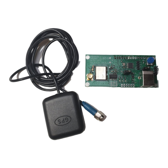
This manual is for the QLG2 GPS/GNSS Receiver module
Firmware version
Contents
1. Introduction....................................................................................................................................................2
2. Getting to know your QLG2............................................................................................................................2
3. Assembly.........................................................................................................................................................5
3.1 Assembly for basic operation....................................................................................................................5
3.2 Use with QCX, U3S, Clock, VFO, ProgRock etc. kits...................................................................................6
3.3 USB connector..........................................................................................................................................6
3.4 USB to Serial converter.............................................................................................................................7
3.5 Powering the board from the USB port..................................................................................................10
3.6 Status LEDs.............................................................................................................................................11
3.7 Fitting an ultracap (a.k.a. supercap)........................................................................................................12
3.8 6-pin interface header............................................................................................................................13
3.9 Jumper wire configuration......................................................................................................................14
3.10 Interface configuration.........................................................................................................................14
3.11 Microcontroller configuration...............................................................................................................16
3.12 Connecting an LCD module...................................................................................................................17
3.13 QLG2 Commands..................................................................................................................................19
4. Firmware update procedure.........................................................................................................................20
5. Circuit diagram (schematic) and description................................................................................................23
6. Testing..........................................................................................................................................................26
7. Acknowledgments........................................................................................................................................27
8. Resources.....................................................................................................................................................27
9. Document Revision history...........................................................................................................................27
1_00.QG2, 1_00a.QG2 and 1_00b.QG2
QLG2 manual for firmware 1.00a
QLG2
GPS/GNSS
Receiver
1
Advertisement
Table of Contents

Related Manuals for QRP Labs QLG2

Summary of Contents for QRP Labs QLG2
-
Page 1: Table Of Contents
QLG2 GPS/GNSS Receiver This manual is for the QLG2 GPS/GNSS Receiver module Firmware version 1_00.QG2, 1_00a.QG2 and 1_00b.QG2 Contents 1. Introduction..............................2 2. Getting to know your QLG2..........................2 3. Assembly.................................5 3.1 Assembly for basic operation........................5 3.2 Use with QCX, U3S, Clock, VFO, ProgRock etc. kits...................6 3.3 USB connector............................6... -
Page 2: Introduction
1. Introduction The QLG2 GNSS (Global Navigation Satellite System) receiver module is an upgrade over the former QLG1 with higher performance and highly flexible features: Multi GNSS satellite constellation receiver supports GPS (US), Galileo (Europe), • GLONASS (Russia) and Beidou (Chinese) - (default GPS + Beidou) - giving a faster more accurate position fix –... - Page 3 Kit contents: Know your QLG2: QLG2 manual for firmware 1.00a...
- Page 4 (firmware update) mode LCD Port: The pinout is in the exact same position as on the QRP Labs Ultimate3S, • Clock or VFO kits; a standard 1602 alphanumeric LCD module can be bolted onto...
-
Page 5: Assembly
Straight out of the box, if you simply install the coaxial connector and plug in the antenna, the QLG2 is backwardly compatible by default with the former QLG1 kit. It is therefore directly compatible with all other QRP Labs kits: QCX-series CW transceivers (QCX, QCX+ and QCX-mini) •... -
Page 6: Use With Qcx, U3S, Clock, Vfo, Progrock Etc. Kits
USB connector For all but the most basic use of the QLG2, you will likely wish to install the USB B connector (supplied) or if you prefer, a micro-USB connector (not supplied). The USB connector is used for two purposes: 1. -
Page 7: Usb To Serial Converter
Note that it does not matter what baud rate you select in the terminal emulator, since USB does not run at any particular rate, and the baud rate of the QLG2 USB to Serial converter is determined by jumpers on the board (see later section). - Page 8 So again, this ensures that the text is all sent in one rapid lump, which is acceptable to the QCX. An example screenshot of the Arduino Serial monitor is shown below, again showing the NMEA sentences scrolling past. QLG2 manual for firmware 1.00a...
- Page 9 You can type the command in full on the Terminal Emulator, and it will be transferred to the GNSS module by the QLG2 USB to Serial converter. A common error is to not calculate the checksum properly; these are the last two characters of the command string.
-
Page 10: Powering The Board From The Usb Port
Powering the board from the USB port In some applications, you may find it convenient to power the QLG2 board from the USB port. In this case, simply solder a jumper wire across JP11 as shown in the diagram below. -
Page 11: Status Leds
Status LEDs Just like it’s predecessor the QLG1, the QLG2 module has the same three LED status LEDs. In the case of QLG2, these are 0603-size SMD LEDs installed on the PCB near the GNSS receiver module. LED 1 (red) is the Power LED and is always lit when QLG2 is powered. -
Page 12: Fitting An Ultracap (A.k.a. Supercap)
Fitting an ultracap (a.k.a. supercap) There is a place on the QLG2 board to fit an ultracap (a.k.a. supercap). This is a lot more reliable means of providing backup power, than the little rechargeable battery on the QLG1. Backup power permits the operation of the internal Real Time Clock (RTC) in the GNSS module and also retains the downloaded satellite ephemeris data, which will enable a hot- start (satellite fix computation) within a second or two of power-up. -
Page 13: 6-Pin Interface Header
6-pin interface header At the center of the QLG2 board’s bottom edge, is a 6-pin header that provides access to the power supply rails, the GNSS outputs, and the Serial port of the USB to Serial converter. The 1pps, Serial data, TXD and RXD signals can be configured to be either 2.8V/3.3V logic level, or 5V logic level. -
Page 14: Jumper Wire Configuration
Jumper wire configuration QLG2 provides a great deal of flexible functionality. Configuration of the module is done by jumper wires, of which there are quite a few on the board. As discussed in the former section headed “Powering the board from the USB port”, you may either solder in actual jumper wires, or pin headers and jumper pin connectors (not supplied). - Page 15 GNSS RXD is connected to the USB to Serial converter transmit signal (DEFAULT) LOWER: GNSS RXD is connected to the RXD pin for external use 6. JP4 is not used currently NOTE: External RXD pin may be 2.8V, 3.3V or 5V logic and is automatically converted. QLG2 manual for firmware 1.00a...
-
Page 16: Microcontroller Configuration
PA0: Baud rate JUMPER: Baud rate is set to 38,400 (suitable for QCX CAT) OPEN: Baud rate is set to 9,600 (suitable for default GNSS module communication) Example configuration for CAT control of a QCX-series CW transceiver: QLG2 manual for firmware 1.00a... -
Page 17: Connecting An Lcd Module
16 pads along the top edge, it will work. The kit is not designed to drive display sizes other than 16 x 2. Installation of the LCD module is on the UNDER-side of the QLG2 module and is done in the same way as on the Ultimate3S, VFO and Clock kits and with the same components,... - Page 18 On power-up, the LCD briefly shows the firmware version of the program file that is held in the Flash memory of the microcontroller chip, for example 1_00.QG2 (the QG2 extension is for QLG2, but because it is a FAT16 file system file names are limited to ye olde 8.3 format).
-
Page 19: Qlg2 Commands
3.13 QLG2 Commands QLG2 normally converts all incoming serial data from the USB host, converts it to standard Serial, and transmits this to the GNSS module (or via the TXD interface pin). However, there are also several commands which you can type into the Terminal Emulator... -
Page 20: Firmware Update Procedure
The connection can easily be made just with a small piece of bare tinned copper wire temporarily inserted in the jumper holes and not soldered; the connection only needs to be made at the moment of power-up of the QLG2, which is when the microcontroller configuration jumpers are read and actioned. - Page 21 QLG2 microcontroller. You may read the file from the QLG2, or write a new one, just by dragging files in your file manager application. On entering the Firmware update procedure, a pop-up window should appear on your PC.
- Page 22 FAT16 format. You may check the properties of the file and will note that it is a 23.5K file. QLG2 firmware images are always a 23.5K file. The creation date and modification date etc. have not been set, because it was important to minimize the size and complexity of the QLG2 QFU bootloader, in order to maximize the space available to the application firmware.
-
Page 23: Circuit Diagram (Schematic) And Description
5. Circuit diagram (schematic) and description QLG2 manual for firmware 1.00a... - Page 24 16 x 12 mm BSS123 Transistor SOT23 R1, R3, R4, R5, R6, Resistor 0603 R8, R9, R13, R14, R15, R16, R17 10-ohms Resistor 0603 Resistor 0603 3.3K Resistor 0603 2.2K Resistor 0603 XTAL 8MHz Crystal 3225 QLG2 manual for firmware 1.00a...
- Page 25 Level conversion from the 2.8V output of the E108-GN01 module, to the 5V logic levels required by other QRP Labs kits, is done using a 74ACT08 quad AND-gate chip; it is not used as an AND gate (all gates have their two inputs tied together), it is simply used as a logic level converter.
-
Page 26: Testing
(to press the pogo pins) using four 25mm nylon spacers. There is a push switch to connect power from the USB connector. The following pictures show the test jig, and then the test jig with QLG2 board under test. QLG2 manual for firmware 1.00a... -
Page 27: Acknowledgments
Test E108-GN01 module using the lab GNSS antenna which is the same model as • supplied in the QLG2 kit, and is lying outside on a sloping tile roof that slopes towards the East. Ensure time-to-first-fix (TTFF) is under 1 minute; on a sample of 20 units, the TTFF •...
Need help?
Do you have a question about the QLG2 and is the answer not in the manual?
Questions and answers