Table of Contents
Advertisement
Quick Links
Track Number: AN0049EN
Version: 0.5
Category: Application Note
Abstract
This document lists the consideration in each step during designing product with MXCHIP module. In order
to achieve rapid mass production, Users should be familiar with the document to pre-consider and avoid problems
effectively in designing, producing, programming and testing.
More Help
For more products information please visit:
For more development data please go to MiCO developer bbs:
For more Fogcloud data please go to Fogcloud developer center:
Copyright Notice
Mxchip copyrights this specification. No part of this specification may be reproduced in any form or
means(specially brand, type name, part number and pictures), without the prior written consent of Mxchip.
9th Floor, No.5, Lane2145 JinshaJiang Road Putuo District, ShangHai.(200333)
User Manual of EMW3239
http://mxchip.com/
Shanghai MXCHIP Information Technology Co., Ltd.
http://mico.io/
http://easylink.io/
Tel.: 021-52655026
Website: http://mxchip.com/
MXCHIP Co., Ltd
2016.12.8
Open
Advertisement
Table of Contents

Subscribe to Our Youtube Channel
Summary of Contents for MXCHIP EMW3239
- Page 1 User Manual of EMW3239 Abstract This document lists the consideration in each step during designing product with MXCHIP module. In order to achieve rapid mass production, Users should be familiar with the document to pre-consider and avoid problems effectively in designing, producing, programming and testing.
-
Page 2: Version Record
Initial document 2016-9-23 Add reference circuit 2016-9-29 Add description of pin function and design consideration Add position figure of PCB 2016-12-2 Add Module downloading method Add module testing method 2016-12-6 2016-12-8 Update format and other problem Design Considerations of EMW3239... -
Page 3: Table Of Contents
Technical Support ..............................19 FCC Statement ................................20 Figure Content Figure 1.1 Top View of EMW3239-P ........................4 Figure 1.2 Top View of EMW3239-E ........................4 Figure 2.1 Top View of Mechanical Size ......................6 Figure 2.2 Side View of Mechanical Size ......................6... - Page 4 Figure 3.9 Position of Routers ........................... 16 Figure 4.1 Stencils size ............................17 Figure 4.2 Temperature Curve of Secondary Reflow ..................17 Table Content Table 2.1 Switch Mode ............................7 Table 3.1Device List ............................12 Table 3.2Download Websites ..........................12 Design Considerations of EMW3239...
- Page 5 [Page 4] 1. Introduction This document lists the consideration in each step during designing product with MXCHIP module. In order to achieve rapid mass production, Users should be familiar with the document to pre-consider and avoid problems effectively in designing, producing, programming and testing.
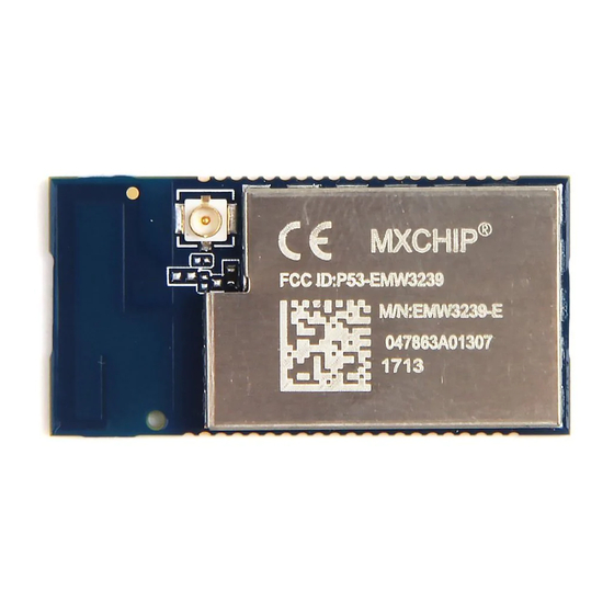
- Page 6 Antenna Technology Antenna Co.,Ltd Antenna Parameter Parameter EMW3239-E EMW3239-P Antenna Type Brass pipe Antenna PCB Antenna Frequency 2400-2500(MHz) 2400-2500(MHz) Impedance 50ohm 50ohm VSWR <2 <2 Antenna gain 2dBI 2dBI Radiation pattern Omnidirectional Omnidirectional Polarization Vertical Vertical Design Considerations of EMW3239...
- Page 7 EMW3239 has 41 pins in two rows (1x20 and 1x21) with 0.8mm pitch. Stamp hole package interface design is used in EMW3239 (as shown in figure 3) to simplify debugging and disassembling for developers, as well as offering varied selection. Also it is benefit for SMT patch and hand-welding.
- Page 8 Datasheet [Page 9] 1.2 Pin Definition 1.2.1 EMW3239 Pin Definition Table 1 Pin Definition of EMW3239 Pins Name Type Multi-select Function User Level √ GPIO BOOT1 √ SPI2_MOSI GPIO TIM12_CH2 I2S2_SD PB15 √ SPI2_NSS GPIO CAN2_RX I2S2_WS PB12 EMW3239...
- Page 9 USART1_TXD PA15 × VBAT VBAT ×DEBUG_IN UART6_RXD GPIO TIM3_CH2 I2S2_CK ( ) Unusable × RESET NRST √ GPIO WAKEUP √ GPIO PC13 √ I2C1_SCL GPIO TIM4_CH3 CAN1_RX √ I2C1_SDA GPIO TIM4_CH4 CAN1_TX √ GPIO TIM2_CH3 I2S2_CK PB10 × × EMW3239...
-
Page 10: Introduction
UART1_TXD GPIO TIM4_CH1 I2C1_SCL √ GPIO JTRST TIM3_CH1 √ USB_ID GPIO TIM1_CH3 PA10 √ GPIO ADC1_5 √ USB_DM GPIO TIM1_CH4 UART1_CTS PA11 ×(BOOT) USB_DP GPIO TIM1_ETR UART1_RTS PA12 ×(STATUS) GPIO ADC1_8 √ GPIO ADC1_4 × 3.3V × 3.3V × EMW3239... - Page 11 7. SWD(pin 25, pin 26) is used to debug and download firmware instead of JTAG; 8. Pins are not available for users with signature “X” while pins with signature “√” is available for users; 9. For other information please contact technical support. EMW3239...
-
Page 12: Considerations In Hardware Design
Mechanical size of EMW3031(Unit: mm) Figure 2.1 Top View of Mechanical Size Figure 2.2 Side View of Mechanical Size Reference Package Design Solder mask openness has the same size with land, as shown in figure2.3(Unit: mm) Design Considerations of EMW3239... -
Page 13: Dc Power Design
The problem rate about final product would be reduced by fully consideration of power design. Pin Function Set module in different mode by combo PIN 36(BOOT), PIN37(STATUS), PIN9(ELINK). Table 2.1 Switch Mode BOOT STATUS ELINK FUNCTION NORMAL WORK BOOTLOADER Design Considerations of EMW3239... - Page 14 Others Pin floating is not allowed in EMW3239. Pin39 and pin 40 is power supply input that could be added a 10uF ceramic capacitors closing to two pins. Power supply is 2.6V to 3.6V. Module could be breakdown if the voltage is over 3.6V.
-
Page 15: Rf Design
The main board PCB should be over 16mm far away from other metal components. Copper, route, closing to metal element is not allowed if the structure needed. P1 to P8 should connect to ground with copper. PCB part below antenna could be hollowed up. Design Considerations of EMW3239... -
Page 16: External Antenna
[Page 10] Figure 2.5 Minimum PCB Clearance Area In order to reduce the influence from metal components to PCB antenna and wireless signal, it is better to mount EMW3239 on four parts. Figure 2.6 Position of the Module 2.5.2 External Antenna Size of external antenna is shown in figure 2.7. -
Page 17: Esd Design
Position of ESD protected components should be reserved if the products require higher ESD requirement such as pins connect to USB and SD-card. EMI should be aware when the module operated by connecting external wire. Using shielding wire or reserving common mode choke could avoid EMI. Design Considerations of EMW3239... -
Page 18: Downloading Firmware And Storage Test Method
Firmware program is sent by FAE of MXCHIP or client which is 600K (application code). ‘Test.bin’ is shown in this note. Switch set up in Downloading Mode 3 switches on develop board of EMW3239 are shown in figure 3.1. Set Easylink as high, STATUS as high and BOOT as L. Design Considerations of EMW3239... -
Page 19: System Connection
Serial Port Selection Find COM number of develop board connect to PC, such as COM4 in figure 3.3. (Note: Enhanced COM Port must be used in serial number). Figure 3.3 Name in Device Manager J-Flash Install ‘Setup_JLink_V600i.exe’. Design Considerations of EMW3239... -
Page 20: J-Flash Set Up
‘JFlash V6.00’ would be found after installing. Figure 3.5 J-Flash signature J-Flash Set Up Use ‘ALT+F7’ or open ‘Options’ then click ‘project settings’. Select ‘SWD’ in Target Interface, ‘ST STM32F412RG’ in MCU, ‘Start application’ in Production. Figure 3.6 Target Interface Set Up Design Considerations of EMW3239... -
Page 21: Testing
Click ‘OK’ after set up. There would be no more set up in following downloading if save the set up. Testing 3.7.1 Environment Set Up Turn on 5 routers that randomly located around test module in a range of 2 to 5 meters. Design Considerations of EMW3239... -
Page 22: Important Statement
Figure 3.9 Position of Routers Important Statement MXCHIP has a duty to make sure there is no quality problem when sell the module to customers. Customers have the rights to ask MXCHIP to exchange goods if the product has quality problem. -
Page 23: Smt
Pseudo soldering could be reduced by control the furnace with temperature curve of secondary reflow, as shown in figure 4.2. Secondary reflow times less than 2 Peak temperature: 250℃ Figure 4.2 Temperature Curve of Secondary Reflow Design Considerations of EMW3239... -
Page 24: Mass Production Test And Product Update
Module Test In order to avoid inferior module and make sure the correct of downloading firmware, MXCHIP strongly suggests product testing before produce. Fully test is required after producing. 5.1.1 Half Secondary Development of Firmware Module connects the MCU from customer through serial port. -
Page 25: Technical Support
Application Note [Page 19] 6. Technical Support For consultation or purchase the product, please contact Mxchip during working hours: From Monday to Friday, morning 9:00~12:00, afternoon 13:00~18:00 Telephone: +86-21-52655026 Contact address: 9 Floor, No.5, Lane2145 JinshaJiang Road Putuo District, ShangHai. -
Page 26: Fcc Statement
When this modular approved transmitter is integrated into a final host device, and the FCC ID is not visible from the outside, than the host device must be labeled with an auxiliary label stating “Contains FCC ID: P53-EMW3239”. Following statement shall be placed on the final host device: “This device complies with part 15 of the FCC Rules.
Need help?
Do you have a question about the EMW3239 and is the answer not in the manual?
Questions and answers