Table of Contents
Advertisement
Quick Links
SERVICE MANUAL
Sec. 1: Main Section
I Specifications
I Preparation for Servicing
I Adjustment Procedures
I Schematic Diagrams
I CBA's
I Exploded views
I Parts List
VIDEO CASSETTE RECORDER
DVD PLAYER &
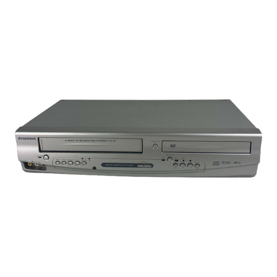
SRD4900
Sec. 2: Deck Mechanism Section
I Standard Maintenance
I Alignment for Mechanism
I Disassembly/Assembly of Mechanism
I Alignment Procedures of Mechanism
I Deck Exploded Views
I Deck Parts List
Advertisement
Chapters
Table of Contents

Related Manuals for Sylvania SRD4900


Summary of Contents for Sylvania SRD4900
- Page 1 I Alignment for Mechanism I Adjustment Procedures I Disassembly/Assembly of Mechanism I Schematic Diagrams I Alignment Procedures of Mechanism I CBA’s I Deck Exploded Views I Exploded views I Deck Parts List I Parts List DVD PLAYER & VIDEO CASSETTE RECORDER SRD4900...
- Page 2 IMPORTANT SAFETY NOTICE Proper service and repair is important to the safe, reliable operation of all Funai Equipment. The service procedures recommended by Funai and described in this service manual are effective methods of performing service operations. Some of these service special tools should be used when and as recommended.
-
Page 3: Table Of Contents
MAIN SECTION DVD PLAYER & VIDEO CASSETTE RECORDER SRD4900 Sec. 1: Main Section I Specifications I Preparation for Servicing I Adjustment Procedures I Schematic Diagrams I CBA’s I Exploded Views I Parts List TABLE OF CONTENTS Specifications................1-1-1 Laser Beam Safety Precautions. -
Page 4: Specifications
SPECIFICATIONS < VCR Section > Description Unit Minimum Nominal Maximum Remark 1. Video 1-1. Video Output (PB) Vp-p SP Mode 1-2. Video Output (R/P) Vp-p SP Mode, 1-3. Video S/N Y (R/P) W/O Burst 1-4. Video Color S/N AM (R/P) SP Mode 1-5. - Page 5 < DVD Section > ITEM CONDITIONS UNIT NOMINAL LIMIT 1. Video Output 75 ohm load ± 0.1 2. Coaxial Digital Out 75 ohm load mVpp ± 50 3. Audio (PCM) 3-1. Output Level 1 kHz 0 dB Vrms 3-2. S/N 3-3.
-
Page 6: Laser Beam Safety Precautions
LASER BEAM SAFETY PRECAUTIONS This DVD player uses a pickup that emits a laser beam. Do not look directly at the laser beam coming from the pickup or allow it to strike against your skin. The laser beam is emitted from the location shown in the figure. When checking the laser diode, be sure to keep your eyes at least 30cm away from the pickup lens when the diode is turned on. -
Page 7: Important Safety Precautions
IMPORTANT SAFETY PRECAUTIONS Product Safety Notice I. Also check areas surrounding repaired locations. J. Be careful that foreign objects (screws, solder Some electrical and mechanical parts have special droplets, etc.) do not remain inside the set. safety-related characteristics which are often not evi- K. - Page 8 Safety Check after Servicing Examine the area surrounding the repaired location for damage or deterioration. Observe that screws, parts, Chassis or Secondary Conductor and wires have been returned to their original posi- tions. Afterwards, do the following tests and confirm the specified values to verify compliance with safety Primary Circuit Terminals standards.
-
Page 9: Standard Notes For Servicing
STANDARD NOTES FOR SERVICING Circuit Board Indications Pb (Lead) Free Solder When soldering, be sure to use the Pb free solder. 1. The output pin of the 3 pin Regulator ICs is indi- cated as shown. How to Remove / Install Flat Pack-IC Top View Bottom View 1. - Page 10 3. The flat pack-IC on the CBA is affixed with glue, so With Soldering Iron: be careful not to break or damage the foil of each (1) Using desoldering braid, remove the solder from all pin or the solder lands under the IC when removing pins of the flat pack-IC.
- Page 11 2. Installation With Iron Wire: (1) Using desoldering braid, remove the solder from all (1) Using desoldering braid, remove the solder from pins of the flat pack-IC. When you use solder flux the foil of each pin of the flat pack-IC on the CBA so which is applied to all pins of the flat pack-IC, you you can install a replacement flat pack-IC more can remove it easily.
- Page 12 Instructions for Handling Semi-conductors Electrostatic breakdown of the semi-conductors may occur due to a potential difference caused by electro- static charge during unpacking or repair work. 1. Ground for Human Body Be sure to wear a grounding band (1MΩ) that is prop- erly grounded to remove any static electricity that may be charged on the body.
-
Page 13: Preparation For Servicing
PREPARATION FOR SERVICING How to Enter the Service Mode About Optical Sensors Caution: An optical sensor system is used for the Tape Start and End Sensors on this equipment. Carefully read and follow the instructions below. Otherwise the unit may operate erratically. What to do for preparation Insert a tape into the Deck Mechanism Assembly and press the PLAY button. -
Page 14: Cabinet Disassembly Instructions
CABINET DISASSEMBLY INSTRUCTIONS 1. Disassembly Flowchart REMOVAL This flowchart indicates the disassembly steps to gain REMOVE/*UNHOOK/ LOC. PART Fig. access to item(s) to be serviced. When reassembling, UNLOCK/RELEASE/ Note follow the steps in reverse order. Bend, route, and UNPLUG/DESOLDER dress the cables as they were originally. DVD Main (S-6), *CN201, [1] Top Case... - Page 15 Reference Notes CAUTION 1: Locking Tabs (L-1) and (L-2) are fragile. Be careful not to break them. (S-1) [1] Top Case 1-1. Release three Locking Tabs (L-1). 1-2. Release three Locking Tabs (L-2), then remove the Front Assembly. CAUTION 2: Electrostatic breakdown of the laser diode in the optical system block may occur as a potential difference caused by electrostatic charge accumulated on cloth, human body etc, during...
- Page 16 CN401 (S-3) (S-7) CN601 (S-7) (S-3) [4] DVD Mecha Assembly (S-3) (S-5) (S-4) (S-7) [6] Loader Holder (S-8) [8] VCR Chassis Unit [5] Partition Plate Fig. D3 Fig. D5 (S-6) [7] DVD Main CBA Unit CN301 CN201 DVD Mecha Short the three short lands by soldering. (Either of two places.) Connector View for A...
- Page 17 Cylinder Assembly FE Head ACE Head Assembly [9] Deck Assembly SW512 LD-SW (S-11) [11] Main CBA [9] Deck Assembly Cam Gear (S-9) [11] Main CBA Hole [10] DVD Shaft (S-10) Open/Close CBA Hole Desolder LD-SW Lead with [11] Main CBA blue stripe From From...
- Page 18 HOW TO EJECT MANUALLY 1. Remove the Top Case. 2. Rotate the roulette in the direction of the arrow as shown below. 3. Pull the tray slowly with a hand. View for A Rotate this roulette in the direction of the arrow DVD Mecha 1-6-5 H9602DC...
-
Page 19: Electrical Adjustment Instructions
ELECTRICAL ADJUSTMENT INSTRUCTIONS General Note: "CBA" is an abbreviation for "Circuit Board Assembly." NOTE: Figure 1 1.Electrical adjustments are required after replacing circuit components and certain mechanical parts. It is important to do these adjustments only after EXT. Syncronize Trigger Point all repairs and replacements have been com- pleted. -
Page 20: Firmware Renewal Mode
FIRMWARE RENEWAL MODE 1. Turn the power on and remove the disc on the tray. 5. After programming is finished, the tray opens auto- 2. To put the DVD player into version up mode, press matically. Fig. e appears on the screen and the [9], [8], [7], [6], and [SEARCH MODE] buttons on checksum in (*3) of Fig. -
Page 21: Block Diagrams
BLOCK DIAGRAMS Servo / System Control Block Diagram 1-9-1 H9602BLS... - Page 22 Video Block Diagram 1-9-2 H9602BLV...
- Page 23 Audio Block Diagram H9602BLA 1-9-3...
- Page 24 Hi-Fi Audio Block Diagram H9602BLH 1-9-4...
- Page 25 Power Supply Block Diagram 1-9-5 H9602BLP...
- Page 26 BLOCK DIAGRAMS <DVD SECTION> DVD System Control / Servo Block Diagram 1-9-6 H9602BLSD...
- Page 27 Digital Signal Process Block Diagram 1-9-7 H9602BLD...
- Page 28 DVD Video / Audio Block Diagram 1-9-8 H9602BLVD...
-
Page 29: Function Indicator Symbols
FUNCTION INDICATOR SYMBOLS Note: The following symbols will appear on the indicator panel to indicate the current mode or operation of the VCR. On-screen modes will also be momentarily displayed on the tv screen when you press the operation buttons. Led Mode Indicator Active When reel and capstan mechanism is not... -
Page 30: Schematic Diagrams / Cba's And Test Points
SCHEMATIC DIAGRAMS / CBA’S AND TEST POINTS Standard Notes WARNING Many electrical and mechanical parts in this chassis have special characteristics. These characteristics often pass unnoticed and the protection afforded by them cannot necessarily be obtained by using replace- ment components rated for higher voltage, wattage, etc. - Page 31 LIST OF CAUTION, NOTES, AND SYMBOLS USED IN THE SCHEMATIC DIAGRAMS ON THE FOLLOWING PAGES: 1. CAUTION: FOR CONTINUED PROTECTION AGAINST FIRE HAZARD, REPLACE ONLY WITH THE SAME TYPE FUSE. ATTENTION: POUR UNE PROTECTION CONTINUE LES RISQES D'INCELE N'UTILISER QUE DES FUSIBLE DE MEMO TYPE.
- Page 32 Main 1/8 Schematic Diagram < VCR Section > MAIN 1/8 REC VIDEO SIGNAL PB VIDEO SIGNAL Ref No. Position REC AUDIO SIGNAL PB AUDIO SIGNAL IC501 TRANSISTORS Q501 Q506 CONNECTORS CN501 CN502 CN504 VARIABLE RESISTOR VR501 TEST POINTS TP505 TP513 H9602SCM1 1-10-3 1-10-4...
- Page 33 Main 2/8 & Sensor Schematic Diagram < VCR Section > REC VIDEO SIGNAL DVD VIDEO + PB VIDEO SIGANL MAIN 2/8 Ref No. Position REC AUDIO SIGNAL PB AUDIO SIGNAL TRANSISTORS DVD AUDIO SIGNAL Q503 Q504 Q563 Q565 Q566 Q567 TEST POINTS TP502 TP506...
- Page 34 Main 3/8 Schematic Diagram < VCR Section > REC VIDEO SIGNAL PB VIDEO SIGNAL MAIN 3/8 DVD VIDEO + PB VIDEO SIGNAL REC AUDIO SIGNAL Ref No. Position PB AUDIO SIGNAL IC301 TRANSISTORS Q301 Q302 Q303 Q421 Q422 Q425 Q426 CONNECTOR CL253 TEST POINTS...
- Page 35 Main 4/8 Schematic Diagram < VCR Section > REC Audio Signal PB Audio Signal DVD AUDIO SIGNAL 1-10-9 1-10-10 H9602SCM4...
- Page 36 Main 5/8 Schematic Diagram < VCR Section > MAIN 5/8 Ref No. Position IC1201 IC1402 TRANSISTORS DVD VIDEO SIGNAL DVD AUDIO SIGNAL DATA (AUDIO) SIGNAL Q1201 Q1202 Q1204 Q1351 AA-1 Q1385 CONNECTOR CL1601 1-10-11 1-10-12 H9602SCM5...
- Page 37 Main 6/8 Schematic Diagram < VCR Section > MAIN 6/8 Ref No. Position DVD VIDEO SIGNAL REC VIDEO SIGNAL PB VIDEO SIGNAL REC AUDIO SIGNAL IC751 AE-3 DVD VIDEO + PB VIDEO SIGANL TRANSISTORS Q391 AF-3 PB AUDIO SIGNAL TEST POINTS DVD AUDIO SIGNAL TP751 AF-2...
- Page 38 Main 7/8 & DVD Open/Close Schematic Diagram < VCR Section > MAIN 7/8 Ref No. Position IC1002 AI-4 IC1004 AI-3 TRANSISTORS Q052 AL-4 Q055 AK-3 Q056 AL-3 Q057 AK-3 Q1004 AJ-2 Q1005 AK-2 Q1006 AL-2 Q1011 AI-2 Q2002 AK-1 Q2013 AI-1 CONNECTORS CN1001...
- Page 39 Main 8/8 Schematic Diagram < VCR Section > MAIN 8/8 CAUTION Ref No. Position CAUTION ! NOTE : FOR CONTINUED PROTECTION AGAINST FIRE HAZARD, Fixed voltage ( or Auto voltage selectable ) power supply circuit is used in this unit. The voltage for parts in hot circuit is measured using REPLACE ONLY WITH THE SAME TYPE FUSE.
- Page 40 Main CBA Top View CAUTION ! CAUTION BECAUSE A HOT CHASSIS GROUND IS PRESENT IN THE POWER Fixed voltage ( or Auto voltage selectable ) power supply circuit is used in this unit. FOR CONTINUED PROTECTION AGAINST FIRE HAZARD, SUPPLY CIRCUIT , AN ISOLATION TRANSFORMER MUST BE USED. If Main Fuse (F1001) is blown, check to see that all components in the power supply REPLACE ONLY WITH THE SAME TYPE FUSE.
- Page 41 Main CBA Bottom View MAIN CBA CAUTION CAUTION ! Ref No. Position FOR CONTINUED PROTECTION AGAINST FIRE HAZARD, Fixed voltage ( or Auto voltage selectable ) power supply circuit is used in this unit. REPLACE ONLY WITH THE SAME TYPE FUSE. IC301 If Main Fuse (F1001) is blown, check to see that all components in the power supply ATTENTION : POUR UNE PROTECTION CONTINUE LES RISQES...
- Page 42 DVD Main 1/3 Schematic Diagram < DVD Section > DVD MAIN 1/3 DATA(VIDEO+AUDIO) SIGNAL Ref No. Position IC201 IC202 IC301 IC461 IC462 TRANSISTORS Q251 Q252 Q253 Q254 CONNECTORS CN201 CN301 CN401 1-10-23 1-10-24 H9602SCD1...
- Page 43 DVD Main 2/3 Schematic Diagram < DVD Section > DATA(VIDEO+AUDIO) SIGNAL VIDEO SIGNAL DATA(AUDIO) SIGNAL 1-10-25 1-10-26 H9602SCD2...
- Page 44 IC101 VOLTAGE CHART PIN.NO PLAY STOP PIN.NO PLAY STOP PIN.NO PLAY STOP PIN.NO PLAY STOP PIN.NO PLAY STOP PIN.NO PLAY STOP PIN.NO PLAY STOP PIN.NO PLAY STOP ----- ----- ----- ----- ----- ----- ----- ----- ----- ----- ----- ----- ----- ----- ----- -----...
- Page 45 DVD Main 3/3 Schematic Diagram < DVD Section > DVD MAIN 3/3 Ref No. Position VIDEO SIGNAL DVD AUDIO SIGNAL DATA(AUDIO) SIGNAL IC103 IC501 IC502 IC601 CONNECTOR CN601 H9602SCD3 1-10-29 1-10-30...
-
Page 46: Waveforms
WAVEFORMS NOTE: Input VCR: COLOR BAR SIGNAL (WITH 1KHz AUDIO SIGNAL) (WF1~WF3, WF10, WF11, WF15) DVD: POWER ON (STOP) MODE (WF4~WF6) CD: 1kHz PLAY (WF7~WF9) (TP751 of Main CBA) Pin 8 of CN1601 Pin 14 of CN1601 WF 1 V-OUT E-E VIDEO-Y VIDEO-Y 0.2V... - Page 47 NOTE: Input VCR: COLOR BAR SIGNAL (WITH 1KHz AUDIO SIGNAL) (WF1~WF3, WF10, WF11, WF15) DVD: POWER ON (STOP) MODE (WF4~WF6) CD: 1kHz PLAY (WF7~WF9) (Pin 12 of TU701) WF13 WF10 (Pin 2 of TU701) MOD-A 20mV x 10 0.2msec PLL-DATA 0.1V x 10 2msec (Pin 6 of TU701)
-
Page 48: Wiring Diagram < Vcr Section
WIRING DIAGRAM < VCR SECTION > 1-12-1 H9602WI... -
Page 49: Wiring Diagram < Dvd Section
WIRING DIAGRAM < DVD SECTION > H9602WID 1-12-2... -
Page 50: System Control Timing Charts
SYSTEM CONTROL TIMING CHARTS [ VCR Section ] Mode SW : LD-SW LD-SW Position detection A/D Input voltage Limit Symbol (Calculated voltage) 3.76V~4.50V (4.12V) 4.51V~5.00V (5.00V) 0.00V~0.25V (0.00V) 1.06V~1.50V (1.21V) 0.66V~1.05V (0.91V) 1.99V~2.60V (2.17V) 1.51V~1.98V (1.80V) 3.20V~3.75V (3.40V) 0.26V~0.65V (0.44V) 4.51V~5.00V (5.00V) 2.61V~3.19V... - Page 51 Still/Slow Control Frame Advance Timing Chart 1) SP Mode 18 RF-SW The first rise of RF-SW after a rise in F-AD signal F-AD (Internal Signal) "H" "H" "Z" C-DRIVE "L" "L" Stop detection (T2) Acceleration Detection (T1) Slow Tracking Value PB CTL Reversal Limit Value 20ms...
- Page 52 2) LP/SLP Mode 18 RF-SW The first rise of RF-SW after a rise in F-AD signal F-AD (Internal Signal) "H" "H" "Z" C-DRIVE "L" "L" Stop detection (T2) Acceleration Detection (T1) Slow Tracking Value PB CTL Reversal Limit Value 20ms 27 C-F/R 79 H-A-SW 78 ROTA...
- Page 53 EJECT ST-S/ END-S "OFF" CASS.LOAD LD-FWD 0.2S LD-REV 0.7S LD-FWD 0.4S LD-FWD 0.2S LD-REV 0.2S LD-FWD 0.5S LD-REV STOP(A) PLAY LD-FWD PLAY LD-FWD LD-REV 0.2S LD-FWD PLAY PLAY PAUSE (SLOW) LD-FWD STILL(SLOW) PLAY LD-REV 0.2S LD-FWD PLAY STOP /EJECT LD-REV STOP(A) Fig.
- Page 54 STOP(A) STOP STOP(A) STOP LD-REV LD-REV 0.2S 0.2S LD-FWD LD-FWD STOP STOP /EJECT /EJECT 1.0S 1.0S LD-FWD LD-FWD 0.5S 0.5S LD-REV LD-REV STOP(A) STOP(A) LD-REV LD-REV 0.2S 0.2S LD-FWD LD-FWD STOP STOP /EJECT LD-REV /EJECT LD-REV 1.0S 1.0S LD-FWD LD-FWD 0.5S 0.5S LD-REV...
- Page 55 [ DVD Section ] Tray Close ~ Play / Play ~ Tray Open Tray Disc Disc Tray Play Close Rotation Stop Open 3.3V Tray IN (TL221) Sled Drive 1.65V (TP303) 1.65V Disc Drive (TP301) 1.65V Focus Drive (TP304) Tracking Drive 1.65V (TP302) 1-13-6...
-
Page 56: Ic Pin Function Descriptions
IC PIN FUNCTION DESCRIPTIONS [ VCR Section ] Signal Active Function Name Level IC501( SERVO / SYSTEM CONTROL IC ) 25 OUT HiFi-H- HiFi Audio Head Switching Pulse “H” ≥ 4.5V, “L” ≤ 1.0V DVD- DVD Power Control 26 OUT Signal Active POWER... - Page 57 Signal Active Signal Active Function Function Name Level Name Level Servo Standard RF Conv. ON/OFF 51 OUT VRO Voltage Output 77 OUT VCR/TV Signal (TV="L"/ VCR="H") Servo Standard IN VRI Voltage Input Color Phase Rotary 78 OUT C-ROTA Changeover Signal AVss AVSS Video Head Amp...
- Page 58 [ DVD Section ] IC571 [ PT6313-S-TP ] Signal In/Out Name Function Name FP-CLK Clock Input FP-STB Serial Interface Strobe N.U. Not Used N.U. Not Used Power Supply Out a Out b Out c Out d Segment Output Out e Out h Pull Down Level Out i...
-
Page 59: Lead Identifications
LEAD IDENTIFICATIONS 2SK3543 2SA1175(J,H,F) 2SA1015-GR(TPE2) KIA4558P 2SC2785(J,H,F,K) 2SC1815-BL(TPE2) NJM4558D BA1F4M-T 2SC1815-GR(TPE2) BN1F4M-T 2SC1815-Y(TPE2) KRA103M 2SC2120-Y(TPE2) KRC103M KTC3198(Y,GR) KTA1266(GR) KTC3203(Y) KTA1267(GR,Y) KTC3193(Y) KTC3199(Y,GR,BL) G D S E C B E C B EL817A EL817B MM1637XVBE EL817C 2SC536NF-NPA-AT PT6313-S-TP LTV-817B-F 2SC536NG-NPA-AT LTV-817C-F PS2561A-1(Q,W) BU4053BCF FMG4A T148... -
Page 60: Exploded Views
EXPLODED VIEWS Cabinet 2L071 2L071 2L071 2L021 2L021 2L071 2L021 2L082 L0-9 W006 Sensor CBA 2L021 2L062 2L051 DVD Main Main CBA 2B11 CBA Unit 2L012 CN3001 Sensor CBA 2B15 CN3002 2B16 2B15 2L051 2B15 2L022 2L011 2B15 2B40 2L051 RM2001 2L022 W002... - Page 61 Packing Unit 1-16-3 H9602PEX...
-
Page 62: Mechanical Parts List
MECHANICAL PARTS LIST PRODUCT SAFETY NOTE: Products marked with a # have special characteristics important to safety. Before replacing any of these components, read carefully the product safety notice in this service manual. Don't degrade the safety of the product through improper ser- vicing. -
Page 63: Electrical Parts List
ELECTRICAL PARTS LIST PRODUCT SAFETY NOTE: Products marked with a Ref. No. Description Part No. # have special characteristics important to safety. CHIP CERAMIC CAP . CH J 390pF/50V or CHD1JJ3CH391 Before replacing any of these components, read care- CHIP CERAMIC CAP . CG J 390pF/50V CHD1JJ3CG391 fully the product safety notice in this service manual. - Page 64 Ref. No. Description Part No. Ref. No. Description Part No. C332 ELECTROLYTIC CAP . 1µF/50V M H7 CE1JMAVSL1R0 C441 ELECTROLYTIC CAP . 0.1µF/50V M H7 CE1JMAVSLR10 C333 CHIP CERAMIC CAP . F Z 0.1µF/50V or CHD1JZB0F104 C448 ELECTROLYTIC CAP . 4.7µF/50V M H7 CE1JMAVSL4R7 CHIP CERAMIC CAP .
- Page 65 Ref. No. Description Part No. Ref. No. Description Part No. C493 ELECTROLYTIC CAP . 4.7µF/25V M H7 CE1EMAVSL4R7 C540 CHIP CERAMIC CAP .(MELF) F Z 0.01µF/16V or CZM1CZB0F103 C494 ELECTROLYTIC CAP . 22µF/16V M H7 CE1CMAVSL220 CHIP CERAMIC CAP .(MELF) F Z 0.01µF/16V CZM1CZ30F103 C495 CHIP CERAMIC CAP .(MELF) F Z 0.01µF/16V or CZM1CZB0F103...
- Page 66 Ref. No. Description Part No. Ref. No. Description Part No. ELECTROLYTIC CAP . 100µF/6.3V M CE0KMASTL101 C1461 ELECTROLYTIC CAP . 1µF/50V M H7 CE1JMAVSL1R0 C1042 ELECTROLYTIC CAP . 470µF/6.3V M or CE0KMASDL471 C1462 ELECTROLYTIC CAP . 470µF/6.3V M or CE0KMASDL471 ELECTROLYTIC CAP .
- Page 67 Ref. No. Description Part No. Ref. No. Description Part No. D565 LED(RED) 204HD/E NPQZ00204HDE PHOTOCOUPLER LTV-817C-F NPEC0LTV817F D566 LED(GREEN) 204-10GD/S957 NPQZ10GDS957 IC1002 VOLTAGE REGULATOR PQ070XZ5MZP QSZBA0TSH034 D567 LED(GREEN) 204-10GD/S957 NPQZ10GDS957 IC1004 VOLTAGE REGULATOR BA3948FP-E2 QSZBA0TRM073 D571 LED(RED) 204HD/E NPQZ00204HDE IC1201 IC:OP AMP KIA4558P or NSZBA0SJY004 D701...
- Page 68 Ref. No. Description Part No. Ref. No. Description Part No. TRANSISTOR 2SC536NG-NPA-AT QQSGC536NNPA TRANSISTOR 2SA1175(F) QQSF02SA1175 Q056 TRANSISTOR KTC3203(Y) or NQSY0KTC3203 Q1008 TRANSISTOR KTC3199(Y) NQSY0KTC3199 TRANSISTOR 2SC2120-Y(TPE2) QQSY02SC2120 Q1011 TRANSISTOR KTC3203(Y) or NQSY0KTC3203 Q057 TRANSISTOR KTC3199(BL) or NQS50KTC3199 TRANSISTOR 2SC2120-Y(TPE2) QQSY02SC2120 TRANSISTOR 2SC2785(K) or QQSK02SC2785...
- Page 69 Ref. No. Description Part No. Ref. No. Description Part No. CHIP RES.(1608) 1/10W 0 Ω or CHIP RES.(1608) 1/10W J 18k Ω R043 RRXAZB5Z0000 RRXAJR5Z0183 CHIP RES.(1608) 1/10W 0 Ω CHIP RES.(1608) 1/10W J 10k Ω or RRXAZR5Z0000 R323 RRXAJB5Z0103 CARBON RES.
- Page 70 Ref. No. Description Part No. Ref. No. Description Part No. CHIP RES.(1608) 1/10W J 470 Ω CHIP RES.(1608) 1/10W J 1k Ω RRXAJR5Z0471 RRXAJR5Z0102 CHIP RES.(1608) 1/10W J 2.7k Ω or CARBON RES. 1/4W J 10k Ω R458 RRXAJB5Z0272 R528 RCX4JATZ0103 CHIP RES.(1608) 1/10W J 2.7k Ω...
- Page 71 Ref. No. Description Part No. Ref. No. Description Part No. CHIP RES.(1608) 1/10W J 1.8k Ω or CARBON RES. 1/4W J 100k Ω R593 RRXAJB5Z0182 RCX4JATZ0104 CHIP RES.(1608) 1/10W J 1.8k Ω CARBON RES. 1/6W J 470k Ω or RRXAJR5Z0182 R1039 RCX6JATZ0474 CHIP RES.(1608) 1/10W J 1.8k Ω...
- Page 72 Ref. No. Description Part No. Ref. No. Description Part No. CHIP RES.(1608) 1/10W J 2.2k Ω or CHIP RES.(1608) 1/10W J 10k Ω or R1236 RRXAJB5Z0222 R2003 RRXAJB5Z0103 CHIP RES.(1608) 1/10W J 2.2k Ω CHIP RES.(1608) 1/10W J 10k Ω RRXAJR5Z0222 RRXAJR5Z0103 CHIP RES.(1608) 1/10W J 2.2k Ω...
- Page 73 DVD OPEN/CLOSE CBA Ref. No. Description Part No. TACT SWITCH SKQSAF001A or SST0101AL041 Ref. No. Description Part No. TACT SWITCH TC-1104(H=9.5) SST0101DNG01 DVD OPEN/CLOSE CBA (MCV-C) ---------- MISCELLANEOUS Consists on the following: 2B11 HEAD SHIELD H9600UD 0VM306770 SWITCHES 2B15 BUSH, LED(F) H3700UD 0VM409508 SW2001 TACT SWITCH KSM0614B or...
- Page 74 DECK MECHANISM SECTION DVD PLAYER & VIDEO CASSETTE RECORDER SRD4900 Sec. 2: Deck Mechanism Section I Standard Maintenance I Alignment for Mechanism I Disassembly/Assembly of Mechanism I Alignment Procedures of Mechanism I Deck Exploded Views I Deck Parts List TABLE OF CONTENTS Standard Maintenance.
-
Page 75: Standard Maintenance
STANDARD MAINTENANCE Service Schedule of Components This maintenance chart shows you the standard of replacement and cleaning time for each part. Because those may replace depending on environment and purpose for use, use the chart for reference. H: Hours : Cleaning I: Replace Deck Periodic Service Schedule... - Page 76 Cleaning Cleaning of ACE Head Clean the head with a cotton swab. Cleaning of Video Head Procedure Clean the head with a head cleaning stick or chamois 1.Remove the top cabinet. cloth. 2.Dip the cotton swab in 90% isopropyl alcohol and Procedure clean the ACE Head.
-
Page 77: Service Fixtures And Tools
SERVICE FIXTURE AND TOOLS J-1-1, J-1-2 Ref. No. Name Part No. Adjustment J-1-1 Alignment Tape FL8A Head Adjustment of ACE Head J-1-2 Alignment Tape FL8N Azimuth and X Value Adjustment of ACE Head / (2 Head only) Adjustment of Envelope Waveform FL8NW (4 Head only) Guide Roller Adj. -
Page 78: Mechanical Alignment Procedures
MECHANICAL ALIGNMENT PROCEDURES Explanation of alignment for the tape to correctly run B. Method to place the Cassette Holder in the tape- starts on the next page. Refer to the information below loaded position without a cassette tape on this page if a tape gets stuck, for example, in the 1. - Page 79 1. Tape Interchangeability Alignment Note: To do these alignment procedures, make sure that the Tracking Control Circuit is set to the preset position every time a tape is loaded or unloaded. (Refer to page 2-3-4, procedure 1-C, step 2.) Equipment required: Dual Trace Oscilloscope VHS Alignment Tape (FL8NW) Guide Roller Adj.
- Page 80 1-A. Preliminary/Final Checking and 3. Check to see that the tape runs without creasing at Alignment of Tape Path Take-up Guide Post [4] or without snaking between Guide Roller [3] and ACE Head. (Fig. M3 and M5) Purpose: 4. If creasing or snaking is apparent, adjust the Tilt To make sure that the tape path is well stabilized.
- Page 81 5. To shift the CTL waveform, press CH UP or CH 4. If the envelope is as shown in Fig. M8, adjust the DOWN button on the remote control unit. Then height of Guide Roller [3] (Refer to Fig. M3) so that make sure that the maximum output position of PB the waveform looks like the one shown in Fig.
- Page 82 1-D. Azimuth Alignment of Audio/Con- trol/ Erase Head Purpose: To correct the Azimuth alignment so that the Audio/ Control/Erase Head meets tape tracks properly. Symptom of Misalignment: If the position of the Audio/Control/Erase Head is not properly aligned, the Audio S/N Ratio or Frequency Response will be poor.
-
Page 83: Disassembly/Assembly Procedures Of Deck Mechanism
DISASSEMBLY/ASSEMBLY PROCEDURES OF DECK MECHANISM Before following the procedures described below, be sure to remove the deck assembly from the cabinet. (Refer to CABINET DISASSEMBLY INSTRUCTIONS on page 1-5-1 of Main Section.) All the following procedures, including those for adjustment and replacement of parts, should be done in Eject mode;... - Page 84 REMOVAL INSTALLATION STEP START- REMOVE/*UNHOOK/ /LOC. PART ADJUSTMENT Fig. No. UNLOCK/RELEASE/ CONDITION UNPLUG/DESOLDER [29] [25] Idler Gear DM1, DM14 [30] [29] Idler Arm DM1, DM14 *(L-11) [31] [25] BT Arm DM2, DM14 *(P-6) Loading Arm (SP) (+)Refer to Alignment [32] [25] DM2, DM14 Assembly...
- Page 85 Top View [41] [42] [43] [46] [14] [13] [11] [15] [36] [10] [12] [35] [34] [40] [29] [30] [16] [39] [38] Fig. DM1 Bottom View [20] [33] [32] [24] [26] [27] [25] [23] [28] [22] [21] [31] Fig. DM2 2-4-3 U29NDA...
- Page 86 (S-1) (S-1) (L-1) (L-3) (L-2) (S-1A) (P-1) Installation of [3] and [6] First, insert [6] diagonally in [3] as shown below. Then, install [6] in [3] while pushing (L-1) in a direction of arrow. After installing [6] in [3], confirm that pin A of [3] enters hole A of [6] properly.
- Page 87 (S-4) [46] [47] (L-14) Desolder from bottom (S-3) Lead with White Stripe View for A Belt Fig. DM7 (S-2) [11] (S-4A) (L-4) (P-3) [13] Removal of [11] [12] 1) Remove screw (S-4A). 2) Unhook spring (P-2). [10] Lead with Desolder Release (L-4) while (P-2) Red Stripe...
- Page 88 Installation of [13] and [12] (S-5) [14] (S-6) [16] [13] [15] Hook spring (P-3) up to [12] and [13], then install then to (P-3) the specified position so that [12] will be floated slightly while holding [12] and [13]. (Refer to Fig. A.) [12] Fig.
- Page 89 (S-8) [22] (C-2) (C-1) [23] (L-6) [21] (P-5) [20] Cap Belt (P-5) [28] Installation position of Cap Belt [21] Cap Belt When installing [23], install the spring (P-5) to [28] as shown in the left figure, and then install [23] while Pin on pressing the spring (P-5) to bottom...
- Page 90 Installation of [25] [25] (C-4) Position of Mode Lever when installed Pin of [35] Pin of [31] Pin of [34] (S-9) (L-10) (L-8) (C-3) [27] [24] [28] Bottom View [26] [25] (L-9) [28] Align [25] and [28] as shown. First groove on [28] First tooth on [44] [28] When reassembling [28],...
- Page 91 [36] Break belt (P-7) [34] [40] (P-8) turn [37] (L-12) turn [38] turn [44] [45] Slide [39] [35] Fig. DM17 Fig. DM15 [42] [41] [43] (L-13) Slide Plate (S-11) Fig. DM16 2-4-9 U29NDA...
-
Page 92: Alignment Procedures Of Mechanism
ALIGNMENT PROCEDURES OF MECHANISM The following procedures describe how to align the Alignment 1 individual gears and levers that make up the tape load- Loading Arm (SP) and (TU) Assembly ing/unloading mechanism. Since information about the state of the mechanism is provided to the System Install Loading Arm (SP) and (TU) Assembly so Control Circuit only through the Mode Switch, it is that their triangle marks point to each other as... -
Page 93: Deck Exploded Views
DECK EXPLODED VIEWS Deck Mechanism View 1 Mark Description Floil G-684G or Multemp MH-D (Blue grease) SLIDUS OIL #150 B494 L1467 L1191 B553 B411 B567 L1053 B410 L1051 Chassis Assembly Top View (Lubricating Point) L1322 B501 B560 L1450 L1450 B426 L1466 B121 B126... - Page 94 Deck Mechanism View 2 Mark Description Floil G-684G or Multemp MH-D (Blue grease) B587 B521 B487 SLIDUS OIL #150 B416 B591 SANKOUL FG84M (Yellow grease) B520 B590 B522 L1406 B148 B499 B508 B573 B592 B574 B558 B564 B557 B414 B565 B525 L1151 B417...
- Page 95 Deck Mechanism View 3 Mark Description Floil G-684G or Multemp MH-D (Blue grease) L1321 SLIDUS OIL #150 B347 L1321 B355 B354 B483 L1341 B425 B482 B562 B300 B563 B313 B529 B360 B359 B361 B555 B303 Some Ref. Numbers are not in sequence. B514 2-6-3 U29N4HDEX...
-
Page 96: Deck Parts List
DECK PARTS LIST Ref.No Description Part No. B521 REV BRAKE SPRING MK12 0VM414222 Ref.No Description Part No. B522 TG POST ASSEMBLY MK11 0VSA12080 CYLINDER ASSEMBLY MK12.5 NTSC 6HD N2268CYL B525 LDG BELT MK11 0VM412804 LOADING MOTOR ASSEMBLY MK12.5 0VSA14636 B529 CLEANER ASSEMBLY MK10 0VSA11161 SLIDE PLATE MK12.5... - Page 97 Printed in Japan 2004-04-07 HO...
Need help?
Do you have a question about the SRD4900 and is the answer not in the manual?
Questions and answers