
Related Manuals for Quectel LTE-A&5G Series

Summary of Contents for Quectel LTE-A&5G Series
- Page 1 PCIe Card EVB User Guide LTE-A&5G Module Series Version: 1.1 Date: 2020-12-26 Status: Released www.quectel.com...
- Page 2 To the maximum extent permitted by law, Quectel excludes all liability for any loss or damage suffered in connection with the use of the functions and features under development, regardless of whether such loss or damage may have been foreseeable.
- Page 3 PCIe Card EVB User Guide Copyright The information contained here is proprietary technical information of Quectel. Transmitting, reproducing, disseminating and editing this document as well as using the content without permission are forbidden. Offenders will be held liable for payment of damages. All rights are reserved in the event of a patent grant or registration of a utility model or design.
-
Page 4: About The Document
LTE-A&5G Module Series PCIe Card EVB User Guide About the Document Revision History Version Date Author Description 2020-09-15 Archibald JIANG Initial Deleted the EM161R-GL in Table 1. Added the switch S104 in Chapter 2.1, Chapter 2020-12-26 Archibald JIANG 2.2 and Chapter 4.6. Updated Figures 1, 4, 6, 8, 15, 16, 19, and 31. -
Page 5: Table Of Contents
LTE-A&5G Module Series PCIe Card EVB User Guide Contents About the Document ..........................3 Contents ..............................4 Table Index ..............................5 Figure Index ..............................6 Introduction ............................7 1.1. Safety Information ........................8 General Overview ..........................9 2.1. Key Features ..........................9 2.2. - Page 6 LTE-A&5G Module Series PCIe Card EVB User Guide Table Index Table 1: Applicable Modules ......................... 7 Table 2: Key Features of PCIe Card EVB ....................9 Table 3: Component Functions of PCIe Card EVB ..................10 Table 4: Accessories List ..........................13 Table 5: Pin Assignment of J401 ........................
- Page 7 LTE-A&5G Module Series PCIe Card EVB User Guide Figure Index Figure 1: Overview of PCIe Card EVB Interface ..................10 Figure 2: PCIe Card EVB Top View ......................12 Figure 3: EVB Kit Accessories ........................13 Figure 4: PCIe Card EVB and Accessories Assembly ................15 Figure 5: EVB Power Supply Block Diagram .....................
-
Page 8: Introduction
LTE-A&5G Module Series PCIe Card EVB User Guide Introduction This document introduces Quectel evaluation board for PCIe cards, the assistant tool for engineers to develop and test Quectel modules, and how to use it. Table 1: Applicable Modules Module Series... -
Page 9: Safety Information
The following safety precautions must be observed during all phases of operation, such as usage, service or repair of any cellular terminal or mobile incorporating Quectel modules. Manufacturers of the cellular terminal should notify users and operating personnel of the following safety information by incorporating these guidelines into all manuals of the product. -
Page 10: General Overview
LTE-A&5G Module Series PCIe Card EVB User Guide General Overview Quectel supplies PCIe Card EVB to engineers to help with the application development. This chapter offers an overview of this EVB. 2.1. Key Features The following table describes the detailed features of PCIe Card EVB. -
Page 11: Interface Overview
LTE-A&5G Module Series PCIe Card EVB User Guide 2.2. Interface Overview J501 Power Switch S103 S104 J802 J101 ANT_MAIN ANT_MIMO1 (U)SIM1 J301 M.2 Module J603 J302 J103 J102 (U)SIM2 ANT_MIMO2 J602 POWER WWAN_LED D102 D101 ANT_DIV S101 J801 S102 J601 J803 DBG_UART USB Type-B... - Page 12 LTE-A&5G Module Series PCIe Card EVB User Guide External power supply J803 Typical supply voltage: +3.7 V PCIe card interface J501 Typical supply voltage: +3.3 V Power Switch S103 VCC ON/OFF control Power key PWRKEY S101 Turn on/off the module Reset button (push button) RESET S102...
-
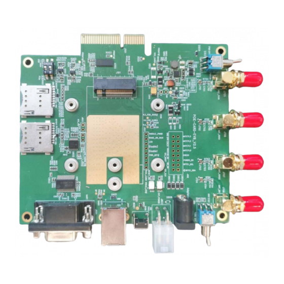
Page 13: Top View Of Pcie Card Evb
LTE-A&5G Module Series PCIe Card EVB User Guide 2.3. Top View of PCIe Card EVB The top view of the PCIe Card EVB is shown below. Figure 2: PCIe Card EVB Top View PCIe_Card_EVB_User_Guide 12 / 38... -
Page 14: Evb Kit Accessories
LTE-A&5G Module Series PCIe Card EVB User Guide 2.4. EVB Kit Accessories All accessories of the PCIe Card EVB kit are listed as below. USB to RS-232 Converter Cable Antennas Power Instruction Sheet Adapter Silicone Soft Bolts and Nuts Adapter Driver Disk plug US Adapter... - Page 15 LTE-A&5G Module Series PCIe Card EVB User Guide ⚫ USB 2.0 to RS-232 driver ⚫ USB driver Driver disk ⚫ QUD driver and UDE driver ⚫ Related tools for modules Silicone soft pad Thermal conductive gasket 4 + 4 for the EVB, 6 for Others Bolts and nuts for EVB assembling the module and heat sink...
-
Page 16: Evb And Accessories Assembly
LTE-A&5G Module Series PCIe Card EVB User Guide EVB and Accessories Assembly The following figure shows the assembly of the EVB and its accessories. Figure 4: PCIe Card EVB and Accessories Assembly PCIe_Card_EVB_User_Guide 15 / 38... -
Page 17: Interface Application
The module can be directly powered by an external power source through connecting with the power jack (J803), and this type of power supply is generally used for current consumption test. The following two figures show the simplified power supply block diagram and the power interface of Quectel PCIe Card EVB. J803 J401... - Page 18 LTE-A&5G Module Series PCIe Card EVB User Guide 3.7 V DC Power Supply 5 V DC Power Supply 3.3 V DC Power Supply Figure 6: EVB Power Supply Interface When using the power jack for power supply, the power plug design of the adapter is shown as below.
-
Page 19: Interface (J101)
LTE-A&5G Module Series PCIe Card EVB User Guide 4.2. M.2 Interface (J101) The M.2 interface is designed to accommodate the modules. The module is connected to the EVB via BTB connector J101. This interface allows customers to easily test functionalities of the module or develop applications based on the module. - Page 20 LTE-A&5G Module Series PCIe Card EVB User Guide Figure 9: Pin Assignment of J401 Table 5: Pin Assignment of J401 Pin No. Pin Name VBUS USB_DM USB_DP GND TX- GND GND PCIe_Card_EVB_User_Guide 19 / 38...
- Page 21 LTE-A&5G Module Series PCIe Card EVB User Guide The following figure shows the connection of the module and the USB Type-B receptacle. J401 Module USB_SS_TX_M USB_SS_TX_P USB_SS_RX_M USB_SS_RX_P R1 0R USB_DP USB_DP R2 0R USB_DM USB_DM USB Type-B Figure 10: Diagram for Module and USB Type-B Receptacle Connection PCIe_Card_EVB_User_Guide 20 / 38...
-
Page 22: U)Sim Interfaces (J301/J302)
LTE-A&5G Module Series PCIe Card EVB User Guide 4.4. (U)SIM Interfaces (J301/J302) The PCIe Card EVB has two 8-pin push-push type Micro (U)SIM card (3.0/1.8 V) connectors J301 and J302. Both of them can be used for the modules. The following figure shows the pin assignment and definition of J301 and J302. -
Page 23: Uart Interface (J601)
LTE-A&5G Module Series PCIe Card EVB User Guide USIM_RST (U)SIM card reset USIM_CLK (U)SIM card clock RESERVED Not connected Ground Not connected USIM_DATA (U)SIM card data RESERVED Not connected USIM_DET (U)SIM card insertion detection 4.5. UART Interface (J601) The PCIe Card EVB offers a UART interface: debug UART port J601. This UART interface supports 115200 bps baud rate by default and can be used for Linux console and log output. - Page 24 LTE-A&5G Module Series PCIe Card EVB User Guide The figure and table below illustrate the pin assignment and pin definition of J601. Figure 14: Pin Assignment of J601 Table 7: Pin Definition of J601 Pin No. Pin Name Description Not connected DBG_TXD Debug UART transmit DBG_RXD...
-
Page 25: Switches And Button (S101/S102/S103/S104*)
LTE-A&5G Module Series PCIe Card EVB User Guide 4.6. Switches and Button (S101/S102/S103/S104*) The PCIe Card EVB includes two power switches (S101 and S103), a reset button (S102), and a PCIe/USB switch (S104)*, as shown in the following figures. S101 S102 Figure 15: Switch S101 and Button S102 S103... -
Page 26: Status Indicators (D101/D102)
LTE-A&5G Module Series PCIe Card EVB User Guide NOTE “*” means under development. Currently the PCIe/USB Switch does not work no matter to which side the switch is switched. 4.7. Status Indicators (D101/D102) The PCIe Card EVB provides two status indication LEDs (D101 and D102). The following figure shows the location of these LED indicators. -
Page 27: Test Points (J102/J103/J602/J603/J802)
LTE-A&5G Module Series PCIe Card EVB User Guide 4.8. Test Points (J102/J103/J602/J603/J802) The PCIe Card EVB provides test points which help customers obtain the corresponding waveforms of some signals. The following figures show the test points of J102, J103, J602, J603 and J802. J103 J102 Figure 18: Test Points of J102 and J103... - Page 28 LTE-A&5G Module Series PCIe Card EVB User Guide Table 10: Pin Definition of J102, J103, J602, J603 and J802 J102 Pin No. Pin Name Module Pin No. Description RFFE1_SDA RFFE data I2S_CLK Connected directly to I2S_CLK of the module RFFE1_SCL RFFE clock I2S_DIN Connected directly to I2S_IN of the module...
- Page 29 LTE-A&5G Module Series PCIe Card EVB User Guide WWAN status indicators test point WAKE_ON_WAN 23 Wake up the host MODULE_PIN68 Module pin 68 J602 Pin No. Pin Name Module Pin No. Description TXD_1V8 TXD_1V8 RXD_1V8 RXD_1V8 J603 Pin No. Pin Name Module Pin No.
-
Page 30: Operation Procedures Illustration
LTE-A&5G Module Series PCIe Card EVB User Guide Operation Procedures Illustration This chapter introduces how to use the PCIe Card EVB for testing and evaluation of the module. 5.1. Power on the Module 1. Connect the module to the EVB. Insert the module into the BTB connector (J101) on the EVB, and then fix the module with screws. -
Page 31: Communication
[1]. Figure 20: USB Ports Install and then use the QCOM provided by Quectel to realize communication between the module and the PC. The following figure shows the settings for COM Port on QCOM: select the correct “COM Port” (USB AT Port which is shown in the figure above) and set the correct “Baudrate” (such as 115200 bps). -
Page 32: Communication Via Pcie Interface
Run the driver disk on PC to install the UDE driver and QUD driver. Figure 23: PCIe Ports Install and then use QCOM provided by Quectel to realize communication between the module and the PC. The following figure shows the settings for COM Port on QCOM: select the correct “COM Port”... -
Page 33: Firmware Upgrade
LTE-A&5G Module Series PCIe Card EVB User Guide Figure 24: COM Port Setting Field on QCOM (AT Port Connection) 5.3. Firmware Upgrade 5.3.1. USB Firmware Upgrade via USB The firmware of the module is upgraded via USB port by default, please follow the procedures below to upgrade the firmware with the tool QFlash. -
Page 34: Firmware Upgrade Via Pcie
LTE-A&5G Module Series PCIe Card EVB User Guide 5.3.2. Firmware Upgrade via PCIe To upgrade the firmware of the module via PCIe port, please follow the procedures below. Use QCOM to open Diagnostic Port (COM5), and then check “HEX String”, sending HEX array: 0x4b, 0x65, 0x01, 0x00, 0x54, 0x0f, 0x7e. - Page 35 LTE-A&5G Module Series PCIe Card EVB User Guide Open cmd.exe (Command Prompt) with administrator authority, then, switch to the firehose directory of the version upgrade file. Execute QBHiServer.exe to download prog_firehose_sdx24.mbn. Figure 28: Third Step of Firmware Upgrade via PCIe After the above command is executed, the EDL port will show up after seconds.
-
Page 36: Reset The Module
LTE-A&5G Module Series PCIe Card EVB User Guide 5.4. Reset the Module The RESET is only used in case of emergency. For example, the software does not respond for more than 5 seconds due to serious problems. Press the button S102 (RESET) for 250–600 ms and then release it to reset the module. However, this operation may cause the loss of information stored in the memory as the module will be reinitialized after the reset. -
Page 37: Current Consumption Test
LTE-A&5G Module Series PCIe Card EVB User Guide 5.6. Current Consumption Test The PCIe Card EVB can also be used to test the current consumption of the module after modifications as follows: 1. Remove R814. R814 Figure 30: Location of R814 2. -
Page 38: Appendix References
LTE-A&5G Module Series PCIe Card EVB User Guide Appendix References Table 12: Related Documents Document Name Remark Quectel_LTE&5G_Windows_USB_Drivers_Installation_ Install USB drivers for M.2 module on Guide Windows system Quectel_QCOM_User_Guide User guide for QCOM tool Quectel_QFlash_User_Guide User guide for QFlash tool Table 13: Terms and Abbreviations Abbreviation Description... - Page 39 LTE-A&5G Module Series PCIe Card EVB User Guide Not Connected Personal Computer Printed Circuit Board Pulse Code Modulation Power Output Radio Frequency UART Universal Asynchronous Receiver/Transmitter Universal Serial Bus (U)SIM (Universal) Subscriber Identity Module PCIe_Card_EVB_User_Guide 38 / 38...
Need help?
Do you have a question about the LTE-A&5G Series and is the answer not in the manual?
Questions and answers