Philips HTS4561/12 Service Manual
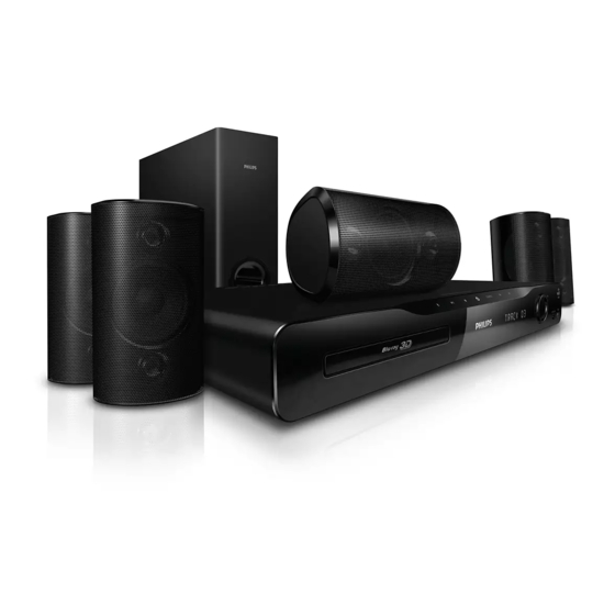
Bd home theater system
Hide thumbs
Also See for HTS4561/12:
- Quick start manual (16 pages) ,
- User manual (52 pages) ,
- Quick start manual (16 pages)
Table of Contents
Advertisement
Quick Links
BD Home Theater System
Service
Service
Service
Service Manual
©
Copyright 2010 Philips Consumer Electronics B.V. Eindhoven, The Netherlands
All rights reserved. No part of this publication may be reproduced, stored in a retrieval system or
transmitted, in any form or by any means, electronic, mechanical, photocopying, or otherwise
without the prior permission of Philips.
Published by
RY_HY1110
Service Audio Printed in The Netherlands Subject to modification
Version 1.0
TABLE OF CONTENTS
Location Of PCB Boards............................................ 1-2
Versions Variation ...................................................... 1-2
Specifications ............................................................ 1-3
Measurement Setup .................................................. 1-6
Service Aids .............................................................. 1-7
ESD & Safety Instruction .......................................... 1-8
Lead-free Soldering Information ................................ 1-9
Setting Procedure & Repair Instructions ...................... 2
Disassembly Instructions & Service Positions .............. 3
Block & Wiring .............................................................. 4
Diagram Quick Strart Guide .......................................... 5
MAIN+VOL Board .......................................................... 6
Power Board .................................................................. 7
BD Board........................................................................ 8
Touch Board .................................................................. 9
Wireless Jack Board .................................................... 10
VFD+USB+MP3+AUX Board ...................................... 11
Mechanical Exploded View.......................................... 12
Revision List ................................................................ 13
1 - 1
Chapter
HTS4561
/12
3139 785 35640
GB
Advertisement
Table of Contents

Related Manuals for Philips HTS4561/12


Summary of Contents for Philips HTS4561/12
- Page 1 Revision List ..............13 © Copyright 2010 Philips Consumer Electronics B.V. Eindhoven, The Netherlands All rights reserved. No part of this publication may be reproduced, stored in a retrieval system or transmitted, in any form or by any means, electronic, mechanical, photocopying, or otherwise without the prior permission of Philips.
-
Page 2: Location Of Pcb Boards
1 - 2 LOCATION OF PCB BOARDS VERSION VARIATION: Type/Versions HTS4561 Features Output Power - 1000W Voltage (220~240V) Wireless ready SERVICE SCENARIO MATRIX: Type/Versions HTS4561 Board in used Main+VOL Board Power Board VFD+USB+MP3+AUX Board BD Board Touch Board Wireless Jack Board *Bd= Board Level Replacement *C = Component Level Repair... -
Page 3: Specifications
1 - 3 SPECIFICATIONS Video formats Media formats If you have a high definition TV, your home • AVCHD, BD, BD-R/ BD-RE, BD-Video, theater allows you to play your video files DVD-Video, DVD+R/+RW, DVD-R/- with: RW, DVD+R/-R DL, CD-R/CD-RW, • Resolution: 1920 x 1080 pixels at Audio CD, Video CD/SVCD, Picture files, •... - Page 4 1 - 4 .mp4 or .m4v files in MP4 container Amplifier • Total output power: Audio Video codec Bit rate codec • Europe and Asia: 1000W RMS (30% THD) AC-3, MPEG 1, MPEG 2 20Mbps (peak • Latin America: 780W (10% THD) MPEG, 40Mbps) •...
- Page 5 1 - 5 • Total output power: Main unit • Europe and Asia: 4 x 135W RMS • Power supply: (30% THD) • Europe/China: 220-240 V~, 50 Hz • Latin America: 4 x 10⁵W RMS (10% • Latin America/Asia Pacific: 110-127 THD) V/220-240 V~, 50-60 Hz •...
-
Page 6: Measurement Setup
1 - 6 MEASUREMENT SETUP Tuner FM Bandpass LF Voltmeter 250Hz-15kHz e.g. PM2534 e.g. 7122 707 48001 RF Generator e.g. PM5326 S/N and distortion meter e.g. Sound Technology ST1700B Use a bandpass filter to eliminate hum (50Hz, 100Hz) and disturbance from the pilottone (19kHz, 38kHz). Use Audio Signal Disc SBC429 4822 397 30184 (replaces test disc 3) -
Page 7: Service Aids
1 - 7 SERVICE AIDS Service Tools: Universal Torx driver holder .........4822 395 91019 Torx bit T10 150mm ...........4822 395 50456 Torx driver set T6-T20 .........4822 395 50145 Torx driver T10 extended ........4822 395 50423 Compact Disc: SBC426/426A Test disc 5 + 5A ......4822 397 30096 SBC442 Audio Burn-in test disc 1kHz ....4822 397 30155 SBC429 Audio Signals disc .........4822 397 30184 Dolby Pro-logic Test Disc ........4822 395 10216... -
Page 8: Class 1 Laser Product
1 - 8 WAARSCHUWING WARNING Alle IC’s en vele andere halfgeleiders zijn All ICs and many other semi-conductors are gevoelig voor electrostatische ontladingen susceptible to electrostatic discharges (ESD). (ESD). Careless handling during repair can reduce life Onzorgvuldig behandelen tijdens reparatie kan drastically. - Page 9 • You will find this and more technical information Use only lead-free solder alloy Philips SAC305 with within the “magazine”, chapter “workshop news”. order code 0622 149 00106. If lead-free solder-paste is required, please contact the manufacturer of your For additional questions please contact your local solder-equipment.
- Page 10 000025.0 version of your home theater with the latest software version (if software updates,please visit available) on the Philips web site, and for BD-Live application and philips.com/support Software BE software update, make sure that the network router has access to the Internet and the firewall is disabled.
- Page 11 2 - 2 2 - 2 c) Assembly Blu-ray Loader to “J800”,”J900”,”J905” on the top of Software upgrade will take 5 minutes BD Board as shown below. Do not switch off! Package version: 000025.0 Software BE Completed Software FE Completed Software MCU1: Not started Software Dock:...
-
Page 12: Repair Instructions
2 - 3 2 - 3 REPAIR INSTRUCTIONS All Functions Power Supply All Functions Touch key has Aux In has MP3 In has MIC In has Tuner has Coaxial In has Optical has Ipod has are not working is not working have no Sound no function no Sound... - Page 13 3 - 1 3 - 1 DISASSEMBLY INSTRUCTIONS Dismantling of theTop & Front Panel Assemble 1) Loosen 6 screws and remove the Top Cover by lifting the rear portion upwards before sliding it out towards the rear. - 4 screws “A” at the back panel as shown in fi gure 1. - 1 screw “B”...
- Page 14 3 - 2 3 - 2 Dismantling of the MP3+USB Board Dismantling of the POWER Board 1) Loosen 2 screws “H” as shown in fi gure 9 to remove MP3+USB Board. 1) Loosen 5 screws “O” on the top of power Board as shown in fi gure 12. Figure 9 Figure 12 Dismantling of the VOL Board and VOL Button...
-
Page 15: Service Positions
3 - 3 3 - 3 SERVICE POSITIONS Figure 15 Dismantling of the AUX Board 1) Loosen 2 screws “M” at the back panel to remove AUX Board as shown in fi gure 16. Note:In some service positions the components or copper patterns of one board may risk touching its neighbouring pc boards or metallic parts. -
Page 16: Block Diagram
4 - 1 4 - 1 BLOCK DIAGRAM... -
Page 17: Wiring Diagram
4 - 2 4 - 2 WIRING DIAGRAM... - Page 18 QUICK START GUIDE The following excerpt of the QSG/DFU serves as an introduction to the set. The complete Direction for Use can be download in the different languages from the internet site of Philips Consumer Care Center:www.support.philips.com. SUB- SUB- FRONT...
- Page 19 5 - 2 5 - 2 FRONT FRONT FRONT REAR REAR SUB- RIGHT LEFT CENTER RIGHT LEFT WOOFER AC 220-240V FRONT FRONT FRONT REAR REAR SUB- ~50Hz RIGHT LEFT CENTER RIGHT LEFT WOOFER DIGITAL IN AUDIO IN COAXIAL AUX 2 OPTICAL Wireless Rear Audio FM(75Ω)
- Page 20 5 - 3 5 - 3 HDMI (ARC) FM (75Ω) ANTENNA MUSIC iLINK AC 220-240V ~50Hz HOME THEATER HOME THEATER HDMI...
- Page 21 5 - 4 5 - 4 MUSIC iLINK DOCK for iPod HOME THEATER...
- Page 22 6 - 1 6 - 1 INTERNAL IC DIAGRAM - CS5346-CQZR LQFP 3.3 V to 5 V 3.3 V ® Left PGA Output ™ I²C /SPI Internal Voltage Control Data Right PGA Output Register Configuration Reference Interrupt Stereo Input 1 Stereo Input 2 Overflow Stereo Input 3...
-
Page 23: Circuit Diagram
6 - 2 6 - 2 CIRCUIT DIAGRAM C1005 D2 C106 C245 C313 C338 C365 C5007A B3 C5044 C3 C5072 C2 C510 C5121A B3 C5155 D3 C5215 C4 CN1009 A1 FB5002 C2 JK5001 B3 Q307 R1038 D2 R1097 D2 R148 R175 R208 R318... -
Page 24: Pcb Layout - Top View
6 - 3 6 - 3 PCB LAYOUT - TOP VIEW C1005 B3 C2901 C2 C323 B2 C351 B1 C386 A2 C5041 C3 C5066 C3 C5090 C3 C5136 A4 C5181 B3 CN1005 C1 FB204 C2 IC305 B1 L5008 C4 Q5002A A2 R1040 C1 R1098 C2 R145 B1... -
Page 25: Pcb Layout - Bottom View
6 - 4 6 - 4 PCB LAYOUT - BOTTOM VIEW C1008 B2 C1015 A2 C1033 A1 C108 C116 C241 C317 C331 C363 C5003 A4 C5010 A4 C507 C5101A B4 C511 C5120A B4 C513 C5157 B3 C701 Q101 R1096 A1 R161 R283 R5007 A4... -
Page 26: Power Board
7 - 1 7 - 1 INTERNAL IC DIAGRAM - AZ431 CATHODE POWER BOARD ANODE TABLE OF CONTENTS Internal IC Diagram ................7-1 Circuit Diagram .................. 7-2 PCB Layout Top View ............... 7-3 PCB Layout Bottom View ..............7-4 INTERNAL IC DIAGRAM - AZ7500BP OUTPUT CTRL Oscillator Pulse-Steering... - Page 27 7 - 2 7 - 2 CIRCUIT DIAGRAM BD901 A1 C924 C947 C960 C970 C985 C999 CY901 B1 D909 D923 IC901 C2 NTC901 C1 Q913 R908 R920 R930C C2 R937 R945H A3 R948 R962 R973 R984 R997 ZD904 A2 C902 C925 C948 C960A C3...
- Page 28 7 - 3 7 - 3 PCB LAYOUT - TOP VIEW BD901 A1 C911 C961 C969 C978 CM901 B1 CX901 C1 D902 D922 F901 IC905 J908 J914 J920 J926 J932 LF901 B1 Q907 R936 R978 TVR902 A1 C901 C915 C962 C970 C985 CN901 C1...
- Page 29 7 - 4 7 - 4 PCB LAYOUT - BOTTOM VIEW C913 C930 C950 C964 C991 D903 D914 IC906 A4 Q915 R904 R914 R922 R930F A2 R938A A4 R945G C3 R945O C3 R954 R963 R972 R983 R990 ZD902 A2 ZD910 B3 C914 C931 C951...
- Page 30 8 - 1 8 - 1 BLOCK DIAGRAM BD BOARD TABLE OF CONTENTS Block Diagram(BD Board) ..............8-1 Voltages for connector pin ..............8-2 Waveforms for measure point ............8-3...
- Page 31 8 - 2 8 - 2 Voltages for per connection pin 6. J800--->>from BD board connect to BD loader(SERVO use) 1. HA500--->>from BD board connect to main board 3. HA501--->>from BD board connect to main board PIN NO PIN Assign Remarks PIN Assign PIN NO...
- Page 32 8 - 3 8 - 3 Waveforms for measure point HA500 PIN10_MIC_IN HA500 PIN9_CEC(no single) HA500 PIN2_Ipod_TX HA500 PIN3_Ipod_RX Disc function wave Play BD Disc wave Play BD Disc wave HA500 PIN12_SCL HA500 PIN13_SDA HA500 PIN5_12C_IRQ HA500 PIN7_IR(VOL up/down) Play BD Disc wave Play BD Disc wave Play BD Disc wave Play BD Disc wave...
- Page 33 8 - 4 8 - 4 Waveforms for measure point HA500 PIN19_BCK HA500 PIN21_AOSDAT0 HA501 PIN4_RX_LRCK HA501 PIN12_RX_MCLK Play BD Disc wave Tuner function wave Play BD Disc wave Tuner function wave HA501 PIN6 RX_BCK HA501 PIN8_RX_DATA0 HA500 PIN22_AOSDAT1 HA500 PIN23_AOSDAT2 Tuner function wave DISC function wave Play BD Disc wave...
- Page 34 8 - 5 8 - 5 Waveforms for measure point HA501 PIN16_ADC_RST CN203 Pin3 USBM pin4 USBP USB and WIFI Function wave...
-
Page 35: Touch Board
9 - 1 9 - 1 TOUCH BOARD TABLE OF CONTENTS Circuit Diagram .................. 9-2 PCB Layout Top & Bottom View ............9-3... - Page 36 9 - 2 9 - 2 CIRCUIT DIAGRAM PWR_LED Standb y SEN 1N SEN 0N SEN 0N PL AY STO P OPEN SEN 1P SEN 1N 3V DD BK3 V3 SEN 0P SEN 0N LED4 PWR_LED R_ 0 LED5 LED4 DA T LED2 LED1...
- Page 37 9 - 3 9 - 3 PCB LAYOUT - TOP VIEW PCB LAYOUT - BOTTOM VIEW RB360 A4...
- Page 38 10 - 1 10 - 1 WIRELESS JACK BOARD TABLE OF CONTENTS Circuit Diagram .................. 10-2 PCB Layout Top & Bottom View ............10-3...
- Page 39 10 - 2 10 - 2 CIRCUIT DIAGRAM CN601 A1 JK601...
- Page 40 10 - 3 10 - 3 PCB LAYOUT - TOP VIEW PCB LAYOUT - BOTTOM VIEW CN601 A1 JK601...
- Page 41 11 - 1 11 - 1 FTD DISPLAY PIN ASSIGNMENT VFD+USB+MP3+AUX BOARD TABLE OF CONTENTS FTD Display Pin Assignment ............. 11-1 Circuit Diagram ................. 11-2 PCB Layout Top & Bottom View ............11-3 PIN CONNECTION...
- Page 42 11 - 2 11 - 2 CIRCUIT DIAGRAM C200 C204 C210 C214 C218 C226 CN256 B1 IC251 Q251 R252 R256 R261 R265 R269 R273 ZD210 C1 C201 C207 C211 C215 C223 C227 DP251 A2 IC251 Q252 R253 R257 R262 R266 R270 RB258 A1 ZD211 C1...
- Page 43 11 - 3 11 - 3 PCB LAYOUT - TOP VIEW C201 C208 C211 CN252 A2 CN256 A1 J258 J260 J262 J265 JK211 Q252 RB258 A3 USB251 A3 C202 C210 C213 CN255 A3 DP251 A1 J259 J261 J263 J266 JK212 Q253 SN251 A1 PCB LAYOUT - BOTTOM VIEW...
- Page 44 12 - 1 12 - 1 Mechanical Exploded View Note: A1=10+11+22+24 B1=9+16 C1=2+3+5+6+7+8+39 27=40+41+42+43+44+45...
-
Page 45: Revision List
13 - 1 REVISION LIST Version 1.0 *Initial release...
Need help?
Do you have a question about the HTS4561/12 and is the answer not in the manual?
Questions and answers