Table of Contents
Advertisement
Quick Links
FM680 User Manual
r1.7
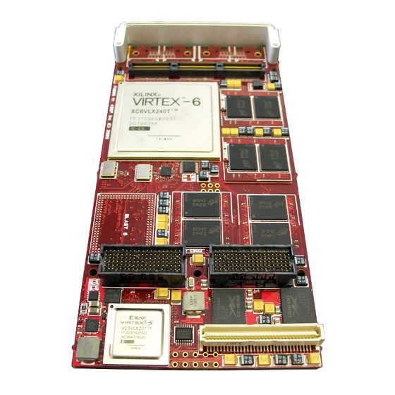
FM680
User Manual for Virtex-6
XMC card
Abaco Systems, USA
Support Portal
This document is the property of Abaco Systems and may not be copied nor communicated
to a third party without the written permission of Abaco Systems.
© Abaco Systems 2009
FM680
www.abaco.com
Page 1 of 32
Advertisement
Table of Contents

Subscribe to Our Youtube Channel
Related Manuals for abaco systems FM680


Summary of Contents for abaco systems FM680
- Page 1 User Manual for Virtex-6 XMC card Abaco Systems, USA Support Portal This document is the property of Abaco Systems and may not be copied nor communicated to a third party without the written permission of Abaco Systems. © Abaco Systems 2009 FM680 www.abaco.com...
- Page 2 FM680 User Manual r1.7 Revision History Document Changes Author Peer Quality Date Review Approval Revision r1.0 Initial Release 2009/12/15 r1.1 Minor modifications 2010/01/20 r1.2 Corrected typos 2010/04/23 r1.3 Corrected typos 2010/08/16 r1.4 Added image 10 for the 2010/08/17 JTAG connector location r1.5...
-
Page 3: Table Of Contents
FM680 User Manual r1.7 Table of Contents Acronyms ........................4 Related Documents ..................... 4 General description ..................... 5 Installation ........................6 Requirements and handling instructions ..............6 Firmware and software .................... 6 Design .......................... 6 FPGA devices ......................6 5.1.1 Virtex-5 device family and package .............. -
Page 4: Acronyms
FM680 User Manual r1.7 Acronyms and related documents 1 Acronyms Analog to Digital Converter Digital to Analog Converter Digitally Controlled Impedance Double Data Rate Digital Signal Processing EPROM Erasable Programmable Read-Only Memory FBGA Fineline Ball Grid Array FPDP Front Panel Data Port... -
Page 5: General Description
4 lanes go either to the V6 or to the V5 Figure 1: FM680 block diagram Build on the success of its predecessor boards of the FM48x series the FM680 also uses the BLAST technology. A total of 5 BLAST sites connect directly to the Virtex-6 FPGA. -
Page 6: Installation
Drivers, API libraries and a program example working in combination with a pre-programmed firmware for both FPGAs are provided. The FM680 is delivered with an interface to the Xilinx PCI-e endpoint core in the Virtex-5 device as well as an example VHDL design in the Virtex- 6 device so users can start performing high bandwidth data transfers over the PCI bus right out of the box. - Page 7 FM680 User Manual r1.7 Virtex-5 Virtex-6 (FPGA A) (FPGA B) GPIO GPIO GPIO GPIO GPIO GPIO GPIO Only on LX550T GPIO and SX475T Figure 2: Inter-FPGA Interface By default Abaco delivers a reference design that uses the interfpga bus to allow high speed data transfer and command distribution between the PCIexpress interface in the FPGA A and the FPGA B.
- Page 8 FM680 User Manual r1.7 INTER_FPGA23 BLAST0_VIO BLAST0_VIO AJ15 INTER_FPGA24 BLAST0_VIO BLAST0_VIO AJ16 INTER_FPGA25 BLAST0_VIO BLAST0_VIO AM16 INTER_FPGA26 BLAST0_VIO BLAST0_VIO AN16 INTER_FPGA27 BLAST0_VIO BLAST0_VIO AT16 INTER_FPGA28 BLAST0_VIO BLAST0_VIO AV16 INTER_FPGA29 BLAST0_VIO BLAST0_VIO AW16 INTER_FPGA30 BLAST0_VIO BLAST0_VIO BA16 INTER_FPGA31 BLAST0_VIO BLAST0_VIO BB16...
-
Page 9: Pci-Express Architecture
Abaco can provide a reference design for the 8-lanes connection to the Virtex-6 FPGA. Please consult with your sales contact for more details. The following performances have been recorded with the FM680 transferring data on the bus using the standard Abaco PCIe interface design: ... -
Page 10: Xmc P15 Connector
Figure 3: PCI-express subsystem diagram. NOTE: There is a swap between the PET0TX0 and PET0TX1 on the FM680. 5.4 XMC P15 connector The Table 3 shows the pin out as defined by VITA 42.3. Only the highlighted pins are connected on the FM680. - Page 11 FM680 User Manual r1.7 PET0p0 PET0n0 3.3V PET0p1 PET0n1 VPWR TRST# MRSTI# PET0p2 PET0n2 3.3V PET0p3 PET0n3 VPWR MRSTO# PET0p4 PET0n4 3.3V PET0p5 PET0n5 VPWR +12V PET0p6 PET0n6 3.3V PET0p7 PET0n7 VPWR -12V VPWR PER0p0 PER0n0 MBIST# PER0p1 PER0n1 VPWR...
-
Page 12: Xmc P16 Connector
The Table 5 shows the pin out as defined by VITA 42.3. Only the highlighted pins are connected on the FM680. Table 6 indicates the signals usage and on board connections. Table 5: XMC P15 pin out as per VITA 42.3... -
Page 13: Pn4 User I/O Connector
FM680 User Manual r1.7 5.6 Pn4 user I/O connector The Pn4 connector is connected to the Virtex-5 device. Connector pin Signal name FPGA pin FPGA pin Signal name Connector pin Pn4_IO0 Pn4_IO1 Pn4_IO2 Pn4_IO3 Pn4_IO4 Pn4_IO5 Pn4_IO6 Pn4_IO7 Pn4_IO8 Pn4_IO9... -
Page 14: Serial Flash
Virtex-6 device. For each BLAST site it is possible to choose from the list of available BLAST modules. For more information about the available BLASTs on the FM680 please consult the following page: BLAST modules http://www.4dsp.com/BLAST.htm... -
Page 15: External Io Interfaces
1 of the PCB). It serves as a base for a daughter card and offers I/O diversity to the FM680 PMC. The FPGA I/O banks are powered either by 1.8V or 2.5V via a large 0 ohms resistor (2.5V is the default if not specified otherwise at the time of order). Using the Xilinx DCI termination options to match the signals impedance allows many electrical standards to be supported by this interface. - Page 16 FM680 User Manual r1.7 Connector Signal Signal Connector Name FPGA pin FPGA pin name FP_P0 FP_P1 FP_N0 FP_N1 FP_X0 FP_X1 FP_P2 FP_P3 FP_N2 FP_N3 FP_X2 FP_X3 FP_P4 FP_P5 FP_N4 FP_N5 FP_X4 FP_X5 FP_P6 FP_P7 FP_N6 FP_N7 FP_X6 FP_X7 FP_P8 FP_P9...
- Page 17 FM680 User Manual r1.7 Connector FPGA FPGA Connector Signal Name Signal name FP_P20 FP_P21 FP_N20 FP_N21 FP_X20 FP_X21 FP_P22 FP_P23 FP_N22 FP_N23 FP_X22 FP_X23 FP_P24 FP_P25 FP_N24 FP_N25 FP_X24 FP_X25 FP_P26 FP_P27 FP_N26 FP_N27 FP_X26 FP_X27 FP_P28 FP_P29 FP_N28 FP_N29...
- Page 18 FM680 User Manual r1.7 Connector Signal Signal Connector Name FPGA pin FPGA pin name FP_P37 FP_P38 FP_N37 FP_N38 FP_X40 FP_X41 FP_P39 FP_P40 FP_N39 FP_N40 FP_X42 FP_X43 FP_P41 FP_P42 FP_N41 FP_N42 FP_X44 FP_X45 FP_P43 FP_P44 FP_N43 FP_N44 FP_X46 FP_X47 FP_P45 FP_P46...
-
Page 19: Power Connection To The Front Panel I/O Daughter Card
Lower rate optical transceivers (2.125 GB/s and 1.0625 GB/s) are available in the same form factor. The Figure 4 shows the block diagram of the optical transceivers on the FM680 and Figure 5 shows the location of the optical transceivers on the PCB. Table 14 shows the pin assignments for each serial lane and the optical transceiver it connects to. - Page 20 FM680 User Manual r1.7 Figure 5: Optical transceiver locations Table 14: Optical transceiver MGT connections FPGA Pin Net Name MGT Block Optical transceiver MGT_FP_RXp3 MGT_FP_TXp3 116_3 MGT_FP_RXn3 MGT_FP_RXp3 MGT_FP_RXp2 MGT_FP_TXp2 116_2 MGT_FP_RXn2 MGT_FP_RXp2 MGT_FP_RXp1 MGT_FP_TXp1 116_1 MGT_FP_RXn1 MGT_FP_RXp1 MGT_FP_RXp0 MGT_FP_TXp0...
-
Page 21: Optical Transceiver Mgt Reference Clock
LED 2 No PCI express traffic PCI express traffic PCI express traffic (red) LED 3 n.a. FM680 PCB revision 2 FM680 PCB revision 1 (only when FPGA A (red) firmware revision is 2.3 or higher) Table 16: LED board status FM680 www.abaco.com... - Page 22 FM680 User Manual r1.7 The LEDs are located on side 2 of the PCB in the front panel area. Their locations are depicted in Figure 7. CPLD_LED0 CPLD_LED1 CPLD_LED2 CPLD_LED3 FPGA_LED1 FPGA_LED0 FPGA_LED3 FPGA_LED2 Figure 7: FPGA and CPLD LED locations To turn on a LED drive the signal low.
-
Page 23: Fpga Configuration
FM680 User Manual r1.7 5.11 FPGA configuration 5.11.1 Flash storage The FPGA firmware is stored on board in a flash device. The 512Mbit device is partly used to store the configuration for both FPGAs. In the default CPLD firmware configuration, the Virtex-5 device and the Virtex-6 device are directly configured from flash if a valid bit stream is stored in the flash for each FPGA. - Page 24 FM680 User Manual r1.7 Figure 9: switch (J1) location Default setting. The Virtex-5 device configuration is loaded from the flash at power up. Virtex-5 device safety configuration loaded from the flash at power up. To be used only if the Virtex-5 device cannot be configured or does not perform properly with the switch in the OFF position.
-
Page 25: Jtag
Figure 7. 5.11.3 JTAG A JTAG connector is available on the FM680 for configuration purposes. The JTAG can also be used to debug the FPGA design with the Xilinx Chipscope. A press fit connector is delivered with the board that can be plugged into the connector holes. -
Page 26: Clock Tree
Table 20 : JTAG pin assignment 5.12 Clock tree The FM680 clock architecture offers an efficient distribution of low jitter clocks. Both FPGA devices receive a low jitter 125MHz clock. A low jitter programmable clock able to generate frequencies from 62.5MHz to 255.5MHz in steps of 0.5MHz is also available. -
Page 27: Power Requirements
CDCV1804 Table 21: Miscellaneous clock connections 6 Power requirements The Power is supplied to the FM680 via the XMC Pn5 connector. Several DC-DC converters generate the appropriate voltage rails for the different devices and interfaces present on board. The FM680 power consumption depends mainly on the FPGA devices work load. By using high efficiency power converters, all care has been taken to ensure that power consumption will remain as low as possible for any given algorithm. - Page 28 -12V MGT power supply 1.0V, 1.2V, 2.5V 2.0A, 2.5A, 0.01A respectively Table 22 : Power supply Optionally, the FM680 can be used as a standalone module and is powered via the external power connector. FM680 www.abaco.com Page 28 of 32...
- Page 29 FM680 User Manual r1.7 5v to 1v0 12v to 5v0 EN5396QI LTC3605 - V6 @ 5A Iout - 6A - V5 @ 1A 5v to 1v0 EN5396QI FET 5V0 - V6 @ 5A VPWR - V5 @ 1A BLAST voltage*5...
-
Page 30: External Power Connector For Stand Alone Mode
(FM680-SA). The height and placement of this connector on the PCB breaches the PMC specifications and the module should not be used in an enclosed chassis compliant to PMC specifications if the external power connector is present on board. -
Page 31: Environment
7.2 Convection cooling 600LFM minimum 7.3 Conduction cooling The FM680 can optionally be delivered as conduction cooled PMC. The FM680 is compliant to ANSI/VITA 20-2001 standard for conduction cooled PMC. 8 Safety This module presents no hazard to the user. -
Page 32: Technical Support
FM680 User Manual r1.7 10 Technical support Technical support for all Abaco Product, hardware, software and firmware is available under Abaco Terms and Conditions of Sales ONLY in its original condition AS-SHIPPED unless agreed to by Abaco and documented in writing, prior to any modifications.
Need help?
Do you have a question about the FM680 and is the answer not in the manual?
Questions and answers