Advertisement
Quick Links
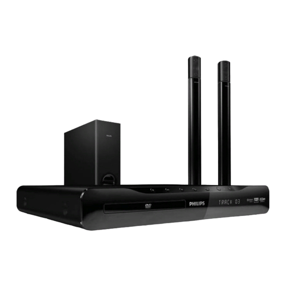
DVD Home Theater System
Service
Service
Service
Service Manual
©
Copyright 2011 Philips Consumer Electronics B.V. Eindhoven, The Netherlands
All rights reserved. No part of this publication may be reproduced, stored in a retrieval system or
transmitted, in any form or by any means, electronic, mechanical, photocopying, or otherwise
without the prior permission of Philips.
Published by
RY_RL1111
Service Audio Printed in The Netherlands Subject to modification
Version 1.0
TABLE OF CONTENTS
Location of PCB Boards ............................................ 1-2
Versions Variation ...................................................... 1-2
Specifications ............................................................ 1-3
Measurement Setup .................................................. 1-4
Service Aids .............................................................. 1-5
ESD & Safety Instruction .......................................... 1-6
Lead-free soldering Information ................................ 1-7
Setting procedure & Repair Instructions........................ 2
Disassembly Instructions & Service positions .............. 3
Quick Start Guide .......................................................... 4
Block & Wiring Diagram ................................................ 5
VFD+USB Board ............................................................ 6
Main Board .................................................................... 7
Power Board .................................................................. 8
Mechanical Exploded view and Packing view ............ 11
Revision List ................................................................ 12
1 - 1
Chapter
HTS2201/
93
3139 785 35700
GB
Advertisement

Related Manuals for Philips HTS2201/93


Summary of Contents for Philips HTS2201/93
- Page 1 Revision List ..............12 © Copyright 2011 Philips Consumer Electronics B.V. Eindhoven, The Netherlands All rights reserved. No part of this publication may be reproduced, stored in a retrieval system or transmitted, in any form or by any means, electronic, mechanical, photocopying, or otherwise without the prior permission of Philips.
- Page 2 1 - 2 LOCATION OF PCB BOARDS VFD PCB USB PCB VERSION VARIATION: Type/Versions HTS2201 Features Output Power - 150W Output Power - 120W Voltage (110-240V) REPAIR SCENARIO MATRIX: HTS2201 Type/Versions Board in used Main Board Power Board VFD+USB Board *C = Component Level Repair...
- Page 3 1 - 3 SPECIFICATIONS Playback media Subwoofer DVD-Video, DVD+R/+RW, DVD-R/-RW, CD-R/CD-RW, Audio Impedance ..............12 ohm CD, Video CD/SVCD, Picture CD, MP3-CD, WMA-CD, DivX- Speaker drivers ........165 mm (6.5”) woofer CD, USB storage device Frequency response ...........20 Hz-150 kHz Dimensions (WxHxD) ......
- Page 4 1 - 4 MEASUREMENT SETUP Tuner FM Bandpass LF Voltmeter 250Hz-15kHz e.g. PM2534 e.g. 7122 707 48001 RF Generator e.g. PM5326 S/N and distortion meter e.g. Sound Technology ST1700B Use a bandpass filter to eliminate hum (50Hz, 100Hz) and disturbance from the pilottone (19kHz, 38kHz). Use Audio Signal Disc SBC429 4822 397 30184 (replaces test disc 3)
- Page 5 1 - 5 SERVICE AIDS Service Tools: Universal Torx driver holder .........4822 395 91019 Torx bit T10 150mm ...........4822 395 50456 Torx driver set T6-T20 .........4822 395 50145 Torx driver T10 extended ........4822 395 50423 Compact Disc: SBC426/426A Test disc 5 + 5A ......4822 397 30096 SBC442 Audio Burn-in test disc 1kHz ....4822 397 30155 SBC429 Audio Signals disc .........4822 397 30184 Dolby Pro-logic Test Disc ........4822 395 10216...
- Page 6 1 - 6 WAARSCHUWING WARNING Alle IC’s en vele andere halfgeleiders zijn All ICs and many other semi-conductors are gevoelig voor electrostatische ontladingen susceptible to electrostatic discharges (ESD). (ESD). Careless handling during repair can reduce life Onzorgvuldig behandelen tijdens reparatie kan drastically.
- Page 7 • You will find this and more technical information Use only lead-free solder alloy Philips SAC305 with within the “magazine”, chapter “workshop news”. order code 0622 149 00106. If lead-free solder-paste is required, please contact the manufacturer of your For additional questions please contact your local solder-equipment.
- Page 8 Press <SETUP> button on R/C. a) Check for the latest software version on b) Select <preference setup> ,then press < OK >. www.philips.com/support. c) Select <default>,then press <OK> to confi rm. Search for your model and click on ‘software&drivers’.
- Page 9 2 - 2 2 - 2 REPAIR INSTRUCTION All function All function Aux in Tuner function DISC function USB is not Power supply is not woring is not sound is not sound is not sound is not sound function is not working All function Aux in Tuner function...
- Page 10 3 - 1 3 - 1 DISASSEMBLY INSTRUCTIONS Dismantling of theTop & Front Panel Assemble 3) Loosen 6 screws and remove the Top Cover by lifting the rear portion upwards before sliding it out towards the rear. - 4 screws “A” at the back panel as shown in fi gure 4. 1) Open the DVD Tray by using the Open/Close Button while the Set is ON and disconnect the mains supply after removing the Tray - 1 screw “B”...
- Page 11 3 - 2 3 - 2 Dismantling of the VFD+USB Board Dismantling of the POWER Board 1) Loosen 7 screws “D” on the top of VFD+USB Board as shown in fi gure 7. 1) Loosen 5 screws “G ” on the top of Power Board as shown in fi gure 10. Figure 7 Dismantling of the MAIN Board 1) Loosen 4 screws “...
- Page 12 4 - 1 CIRCUIT DIAGRAM The following excerpt of the QSG/DFU serves as an introduction to the set. The complete Direction for Use can be download in the different languages from the internet site of Philips Consumer care Center: www.support.philips.com User Manual...
- Page 13 4 - 2 4 - 2...
- Page 14 4 - 3 4 - 3 General Setup OSD Language Screen Saver Auto Standby DivX(R) VOD Code Screen Saver Sleep Timer DivX(R) VOD Code General Setup OSD Language English Screen Saver Auto Standby DivX(R) VOD Code Screen Saver Sleep Timer DivX(R) VOD Code...
- Page 15 4 - 4 4 - 4 User Manual...
- Page 16 5 - 1 5 - 1 BLOCK DIAGRAM...
- Page 17 5 - 2 5 - 2 WIRING DIAGRAM MAIN BOARD CN204 CN201 CN203 CN202 CN302 For 220V input CN902 CN901 POWER BOARD LOADER CN903 For usb input VFD BOARD CN601...
- Page 18 6 - 1 6 - 1 FTD DISPLAY PIN ASSIGNMENT VFD+USB BOARD TABLE OF CONTENTS FTD Display Pin Assignment ............. 6-1 Circuit Diagram ................. 6-2 PCB Layout Top & Bottom View ............6-3 PIN CONNECTION...
- Page 19 6 - 2 6 - 2 CIRCUIT DIAGRAM C601 B1 C604 B1 C607 B2 C610 A2 C613 C1 C616 B2 DP601 A2 Q601 A2 R602 A1 R605 A1 R608 A2 R611 B1 R614 B2 R617 C1 R620 D1 R623 C1 SN601 A2 TA603 A1 TA606 A2...
- Page 20 6 - 3 6 - 3 PCB LAYOUT - TOP VIEW C604 C609 CN602 A1 JM12 LD601 TA601 TA603 TA605 TA607 C608 CN601 A2 DP601 A3 JM10 SN601 A4 TA602 TA604 TA606 USB601 A1 CN602 PCB LAYOUT - BOTTOM VIEW C601 A3 C603 A1 C606 A4...
-
Page 21: Internal Ic Diagram
7 - 1 7 - 1 INTERNAL IC DIAGRAM - MT1389DXE/J Debug CVBS, Y/C 108MHz Port Component Module TV Encoder Video RF Amplifier Video DAC Servo IO Motor Servo Video Drive Processor Processor interlacer Spindle Control FLASH MPEG-1/2/4 Audio JPEG MAIN BOARD Memory Video Decoder... - Page 22 7 - 2 7 - 2 CIRCUIT DIAGRAM - part one C401 D1 C412 C425 C437 D1 C451 C463 C483 C508 C536 D401 C2 FB406 B1 Q402 B1 R410 R421 R438 R449 C1 R460 C2 R472 R495 R517 C402 C413 C426 C438 C1 C452 D2...
- Page 23 7 - 3 7 - 3 CIRCUIT DIAGRAM - part two C201 A2 C209 D3 C217 A3 C225 D4 C234 A1 C242 A1 C250 C1 C259 D1 C267 D2 C275 D1 C283 B1 C291 B4 D211 B1 FB206 D1 FB215 D1 IC205 D2 L207 D3 L215 B1...
- Page 24 7 - 4 7 - 4 CIRCUIT DIAGRAM - part three C2201 C1 C2210 C1 C302 A2 C311 B3 C320 A1 C329 A3 C338 D1 C347 B4 C357 D3 C366 A1 D2202 C1 FB308 D2 IC301 A2 L303 D3 Q306 D4 R2209 B1 R2218 B2 R304 A3...
- Page 25 7 - 5 7 - 5 PCB LAYOUT - TOP VIEW C201 C2213 C1 C247 C283 C323 C361 C420 C460 C524 D408 FB302 A2 IC202 L212 Q301 R214 R2215 C1 R231 R303 R328 R354 R375 R412 R440 TU301 B1 C202 C2215 B1 C249 C284...
- Page 26 7 - 6 7 - 6 PCB LAYOUT - BOTTOM VIEW C203 B1 C212 B1 C241 A1 C259 C3 C270 C2 C303 B3 C330 A2 C339 C4 C365 B3 C411 A3 C434 A3 C482 B5 C512 B5 C557 A5 FB209 C3 L207 B2 R246 B2 R325 A3...
- Page 27 8 - 1 8 - 1 INTERNAL IC DIAGRAM - AZ431 CATHODE POWER BOARD ANODE TABLE OF CONTENTS Internal IC Diagram ................8-1 Circuit Diagram .................. 8-2 PCB Layout Top View ............... 8-3 PCB Layout Bottom View ..............8-4...
-
Page 28: Circuit Diagram
8 - 2 8 - 2 CIRCUIT DIAGRAM BD901 A1 C907 C916 C930 C938 C944 C950 C961 C968 D903 D909 IC901 B1 L902 Q903 R902 R911 R917 R923 R929 R936 R942 R960 T901 ZD904 A2 C902 C910 C917 C932 C939 C945 C951 C962... -
Page 29: Pcb Layout Top View
8 - 3 8 - 3 PCB LAYOUT - TOP VIEW BD901 B1 C910 C917 C938 C950 CN901 D1 D905 D912 J902 J908 J915 L904 Q905 R924 C902 C912 C922 C939 C951 CN902 D4 D906 F901 J903 J909 J916 L905 R906 R930 C903... -
Page 30: Pcb Layout Bottom View
8 - 4 8 - 4 PCB LAYOUT - BOTTOM VIEW C905 C936 C945 C961 D911 Q907 R905 R916 R922 R929 R936 R941 R946 R963 ZD903 A4 C925 C941 C948 C963 IC901 R901 R908 R917 R925 R932 R937 R942 R947 R964 ZD904 A2 C926... - Page 31 9 - 1 9 - 1 Mechanical Exploded View S2 HST143084-1060 SCREW M3.0x0.5PxL6mm NICKEL S3 HST143084-3060 SCREW M3x0.5PxL6mm BLACK OXIDE S5 HSP140054-1060 SCREW T3.0x1.06PxL6mm NICKEL S6 HST143084-1080 SCREW M3.0x0.5PxL8mm NICKEL S7 HSP140054-1080 SCREW T3.0x1.06PxL8mm NICKEL...
- Page 32 9 - 2 9 - 2 Packing View (part one)
- Page 33 9 - 3 9 - 3 Packing View (part two)
- Page 34 10 - 1 REVISION LIST Version 1.0 *Initial release...
Need help?
Do you have a question about the HTS2201/93 and is the answer not in the manual?
Questions and answers