Table of Contents
Advertisement
Quick Links
Advertisement
Table of Contents

Summary of Contents for ABACO FMC30RF
- Page 1 FMC30RF User Manual Abaco Systems, USA Support Portal This document is the property of Abaco Systems and may not be copied nor communicated to a third party without the written permission of Abaco Systems. © Abaco Systems 2015 UM015 www.abaco.com...
- Page 2 FMC30RF User Manual r1.3 Revision History Date Revision Revision 2012-05-30 Draft 2012-05-30 Release after review 2012-10-05 Additional info on LNA and reference oscillator 2014-06-11 Update voltage monitoring section Additional info in Figure 5 and pin out. 2015-02-12 Added RF input analog line-up description, updated RF in/out characteristics.
-
Page 3: Table Of Contents
Time-Division Duplex (TDD) ...................10 Frequency-Division Duplex (FDD) ................10 Multiple-Input Multiple-Output (MIMO) ..............10 Controlling the FMC30RF ...................11 Guidelines for controlling the RF path ..............11 Guidelines for controlling the CDCE62005 .............11 Guidelines for controlling the TRF3765 ..............12 Guidelines for controlling the TRF3711 ..............12 Guidelines for controlling the TRF3720 ..............12... -
Page 4: Acronyms And Related Documents
FMC30RF User Manual r1.3 1 Acronyms and related documents 1.1 Acronyms Analog to Digital Converter Double Data Rate EPROM Erasable Programmable Read-Only Memory FBGA Fineline Ball Grid Array FPGA Mezzanine Card FPGA Field Programmable Gate Array JTAG Join Test Action Group... -
Page 5: General Description
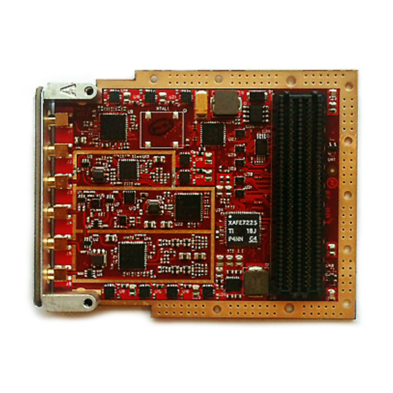
The FMC30RF is an FMC Daughter Card which is fully compliant with the VITA 57.1-2010 standard. The FMC30RF offers in a small footprint a low power and fully featured Rx/Tx signal path for the development and deployment of advanced RF solutions. With a frequency range coverage from 400MHz to 3.0GHz (two ranges) and up to 60MHz bandwidth the FMC30RF... -
Page 6: Phycisal Specifications
The FMC30RF card uses a mix of LVDS and LVCMOS signals. According to the FMC standard VADJ should be +2.5V to support LVDS, but the FMC30RF is designed to accept any level on VADJ ranging between 1.65V and 5.5V. VIO_B_M2C connections are connected to VADJ on the FMC30RF. -
Page 7: Jtag
4.2.2 JTAG The FMC30RF card TDO pin is connected to the TDI pin (through an SN74LVC1G126 buffer) to ensure continuity of the JTAG chain. TCK, TMS and TRST are left unconnected on the FMC30RF. - Page 8 FMC30RF User Manual r1.3 Guidelines of controlling tuneable gain and attenuators are provided in section 6. The maximum input level at the RF input is +3dBm and can be applied to the board when the total gain of the analog line-up is set to minimum. This is done by:...
-
Page 9: Main Characteristic
Input Impedance External Reference Output (REF OUT) Output Level 3.3V (AC coupled LVCMOS) Output Frequency 10MHz – 250MHz Table 2: FMC30RF daughter card main characteristics Make sure minimum gain is configured, refer to section 4.2.4. UM015 www.abaco.com - 9 -... -
Page 10: Modes Of Operation
PRI_REF CDCE62005 REF IN Figure 5: Signal Path 5.1 Time-Division Duplex (TDD) The FMC30RF supports TDD using the RF I/O connector. The RF I/O connector is either receiving (TRX_SWITCH_CTRL=0) transmitting (TRX_SWITCH_CTRL=1). TRX_SWITCH_CTRL signal should be driven by the FPGA trough the FMC connector. -
Page 11: Controlling The Fmc30Rf
6 Controlling the FMC30RF Good knowledge of the internal structure and communication protocol of relevant on-board devices is required for controlling the FMC30RF. This document only provides guidelines for programming the devices. For detailed information it is recommended to refer to the datasheets listed in the related documents section of this document. -
Page 12: Guidelines For Controlling The Trf3765
FMC30RF User Manual r1.3 • CDCE62005_LOCK • CDCE62005_REFEN Refer to Appendix A for a description of these signals. 6.3 Guidelines for controlling the TRF3765 The following control signals connect from the FMC connector to the TRF3765; • SCLK (shared with other devices) •... -
Page 13: Guidelines For Controlling The Amc7823
Refer to Appendix A for a description of these signals. 7 Power supply Power is supplied to the FMC30RF card through the FMC connector. The pin current rating is 2.7A, but the overall maximum as specified by the FMC standard is limited according to Table... -
Page 14: Environment
5.5V à 5.0V TPS74401(148mA) TRF3720_5p0 5.5V à 5.0V TPS74401 (250mA) TRF3720_3p3 3.8V à 3.3V TPS74401 (190mA) TRF3765_3p3 3.8V à 3.3V Figure 7: FMC30RF Power Supply Architecture 8 Environment 8.1 Temperature Operating temperature: • ° ° C to +85 C (Industrial) Storage temperature: UM015 www.abaco.com... -
Page 15: Monitoring
Two different types of cooling will be available for the FMC30RF. 8.3.1 Convection cooling The air flow provided by the chassis fans the FMC30RF is enclosed in will dissipate the heat generated by the on board components. A minimum airflow of 300 LFM is recommended. -
Page 16: Safety
FMC30RF User Manual r1.3 9 Safety This module presents no hazard to the user. 10 EMC This module is designed to operate from within an enclosed host system, which is build to provide EMC shielding. Operation within the EU EMC guidelines is not guaranteed unless it is installed within an adequate host system. -
Page 17: Appendix Alpc Pin-Out Fmc30Rf
Appendix A LPC pin-out FMC30RF FMC label FMC30RF Signal Description CLK0_M2C_N CLK_TO_FPGA_N Output from CDCE62005 CLK0_M2C_P CLK_TO_FPGA_P Output from CDCE62005 LA00_N_CC ADC_DCLKOUT_N Connects to AFE7225 LA00_P_CC ADC_DCLKOUT_P Connects to AFE7225 LA01_N_CC ADC_FCLKOUT_N Connects to AFE7225 LA01_P_CC ADC_FCLKOUT_P Connects to AFE7225... - Page 18 FMC30RF User Manual r1.3 LA15_P AFE7225_RESET Connects to AFE7225 RESET LA16_N AFE7225_CS# Connects to AFE7225 SEN LA16_P AFE7225_PD Connects to AFE7225 PDN LA17_N_CC RF_ATT_V4 Connects to SKY12329-350LF V4 LA17_P_CC RF_ATT_V3 Connects to SKY12329-350LF V3 LA18_N_CC AMC7823_CS# Connects to AMC7823 SS...
- Page 19 FMC30RF User Manual r1.3 LA29_P TRF3711_SDOUT Connects to TRF3711 READBACK LA30_N AMC7823_SDOUT Connects to AMC7823 MISO LA30_P CDCE62005_CS# Connects to CDCE62005 SPI_LE LA31_N AMC7823_GALR# Connects to AMC7823 GALR# LA31_P TRF3765_SDOUT Connects to TRF3765 READBACK LA32_N Not connected LA32_P Not connected...
Need help?
Do you have a question about the FMC30RF and is the answer not in the manual?
Questions and answers