
Related Manuals for VORAGO PEB1

Summary of Contents for VORAGO PEB1
- Page 1 PEB1 USER MANUAL Evaluation board for VA416x0 MCU from VORAGO JUNE 20, 2020 VORAGO TECHNOLOGIES...
-
Page 2: Table Of Contents
Introduction ........................... 2 Purpose of Document ....................2 Overview of Hardware and Software components ............2 Key components included on the PEB1 evaluation kit (subject to change depending on availability)..........................2 PEB1 MCU board component placement diagram ............5 Connector pin assignment table for MCU board ............ -
Page 3: Introduction
Cypress FM22L16 FRAM 1.3.1 The PEB1 MCU board The PEB1 MCU board includes a SEGGER JTAG Probe, the J-Link OB interface. A separate JTAG debug pod is not required however a dedicated connector is provided if a different tool is... - Page 4 Figure 1 - Block diagram of PEB1 1.3.2 The PEB1 GPIO board The PEB1 GPIO board provides additional connectivity to the VA416x0 MCU. Access to all 104 GPIO pins are available on the various convenient headers. Header pins located on the GPIO board as well provide access to integrated board resources, ADC inputs, DAC outputs, I2C interfaces, CAN interfaces with transceivers, and a connector for a SpaceWire interface.
- Page 5 Figure 2 - Block diagram of PEB1 GPIO board 1.3.3 The PEB1 EBI/Ethernet board The PEB1 EBI/Ethernet board provides additional connectivity to the VA416x0 MCU. To suit another example of port expansion, covering a different set of peripherals, the External Bus...
-
Page 6: Peb1 Mcu Board Component Placement Diagram
VA41620/VA41630 Evaluation Board User’s Manual V1.0 1.4 PEB1 MCU board component placement diagram... -
Page 7: Connector Pin Assignment Table For Mcu Board
1.5 Connector pin assignment table for MCU board The schematics for the three boards are included in PEB1 download package. To assist with quickly finding which pins are tied to the various connectors on the board, the following set of tables are provided. -
Page 8: Materials List
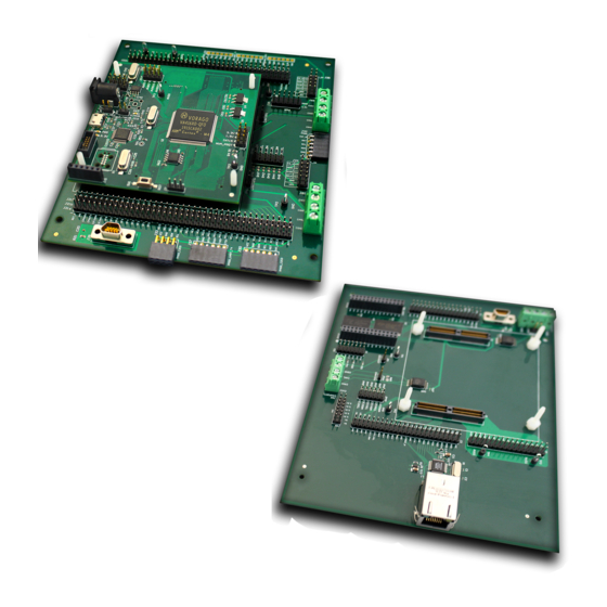
This photo shows the PEB1 MCU board mounted onto the PEB1 GPIO board. The connection between these two boards is made by aligning the plastic pins on the lower board with the holes on the upper board. Similar connectivity is achieved with the PEB1 MCU board and the PEB1 EBI/Ethernet board. -
Page 9: Connector Pin Assignment Table For Gpio Board
VA41620/VA41630 Evaluation Board User’s Manual V1.0 1.8 Connector pin assignment table for GPIO board The GPIO board has two large 0.1in headers, labeled J21 and J22. The connections to the MCU are as follows. - Page 10 VA41620/VA41630 Evaluation Board User’s Manual V1.0 Table 3 - PEB1 GPIO Board Connector designations...
- Page 11 V1.0 Table 4 - PEB1 GPIO Board Connector designations PEB1 EBI/Ethernet board (shown without the PEB1 MCU board attached). The connection between the two boards is made by aligning the plastic pins on the lower board with the holes on the upper board.
- Page 12 VA41620/VA41630 Evaluation Board User’s Manual V1.0...
- Page 13 VA41620/VA41630 Evaluation Board User’s Manual V1.0 Table 5 - PEB1 EBI/Ethernet Board Connector designations...
-
Page 14: Support
VA416x0 MCU. Keys pressed on the keyboard can be routed to the VA416x0 MCU and printf statements from the VA416x0 MCU can either be logged into a file or shown on a terminal window. See Figure 3 - Software interaction for PEB1. -
Page 15: Required Downloads
The following downloads are required to allow full functionality of the evaluation board. These tools are evaluation versions and are free of charge. Please download the Keil IDE, the Segger J- Link software and the VORAGO PEB1 software development code as outlined in the below sections. - Page 16 VA41620/VA41630 Evaluation Board User’s Manual V1.0 Please use the default directories for the “core” and “pack” when prompted for information during the install.
- Page 17 2.1.2 Segger J-Link https://www.segger.com/jlink-software.html Select Software and documentation pack for Windows V6.10n [23,162 KB]. If a later version is available, please use it. 2.1.3 VORAGO Software and Documentation http://voragotech.com/PEB1. This will have the following components in a single .zip file:...
-
Page 18: Hardware Check
MCU voltage 3.3v and 1.5v supply shunts on JP4 (pin 5 to 6 and pin 7 to 8) o Analog voltage supply connections on JP15 (all four jumpers in place) • Connect the USB cable between PC and the PEB1 board o The green DS1 LED will indicate that power is applied to the board. - Page 19 VA41620/VA41630 Evaluation Board User’s Manual V1.0 Command Arguments Comments Provides list of all available commands $help none $help $readport [port 0-6] [mask] – Masked pins input, read IO port $setport [port 0-6] [mask] [val] - Set masked pins hi/loon Port output 1 or 0 $readadc [ch 0-15] - Readan ADC channel $setdac [0 or 1] [0x0 –...
- Page 20 VA41620/VA41630 Evaluation Board User’s Manual V1.0 Response: $OK $rom1rd [addr] Reads one address location from the SPI boot the FRAM device. Example: $rom1rd 0x0 Response: $OK 0x00000000 $auxwr [addr] [data32] Writes one address location of the external FRAM device. Example: $auxwr 0x0 0x0 Response: $OK $auxrd [addr]...
-
Page 21: J-Link Ob And Rtt (Real Time Terminal)
Device will lose its connection to the J-Link RTT terminal and will have to be reconnected. 4.1 J-Link OB and RTT (Real Time Terminal) Inside the PEB1 demonstration program, there is a series of subroutines provided by Segger to configure the RTT, transmit and receive characters. Inside of this code, buffers are created and the RTT Control Block address is fixed at 0x1FFFF000. - Page 22 VA41620/VA41630 Evaluation Board User’s Manual V1.0 4.1.1 RTT Client application Included in the Segger download is an application titled “J-LINK RTT Viewer”. This application allows information sent from the MCU to be either displayed on a terminal or logged into a file. Alternatively, data from the keypad of the PC can be sent to the MCU. When the application is first opened, a dialog box is shown that allows the user to configure the connection.
- Page 23 VA41620/VA41630 Evaluation Board User’s Manual V1.0 Entering the $help command will produce the following results: 4.1.2 Starting and Stopping RTT Viewer Starting the viewer can occur at any time during a debug session. However, after the Viewer is connected and the MCU exits a debug session, the viewer will error out since the host software...
-
Page 24: Starting An Ide And Building A Program
A virtual serial communication cable such as FTDI “TTL-232R-3V3-WE” or SparkFun USB to RS232-TTL (https://www.sparkfun.com/products/12731) can be used to connect a PC to the board. PORTG[0] and PORTG[1] are available on connector J7 of the PEB1 board. 5 Starting an IDE and building a program Depending upon which IDE you decide to use, the steps to run a program will be different. - Page 25 VA41620/VA41630 Evaluation Board User’s Manual V1.0 Double click on the file ending with uvprojx and the Keil IDE should open with this project loaded. The screen should look like the figure below.
- Page 26 From the Project pull-down menu, select “manage” and then “pack installer”. This will open another window. - From the pack installer window, Use the “file” pull-down menu and select “import”. Navigate to the VA416xx1.0.0.pack file which was part of the VORAGO download and hit the Open button.
- Page 27 MCU and SWD debugger probe. The following sections provide the minimum options for the VORAGO software development kit to function. All the options can be accessed under the Project pull-down menu as shown here. An...
- Page 28 The Keil IDE supports many forms of interfaces. The default debug connection is the ULINK2 from Keil. The PEB1 board has a built in SWD interface called Segger J-Link OB. The IDE must be told which interface is used. See below for screen captures on how to do this. First use the pull-down menu of the Debug options window to select “J-LINK/J-TRACE Cortex”.
- Page 29 VA41620/VA41630 Evaluation Board User’s Manual V1.0 Second, set the J-Link to use the SWD connection. Click the Settings button and select “SWD” in the Port Window. The “Max Clock” selection can be anything up to 5 MHz. The board should be connected to a PC prior to setting up the Debugger.
- Page 30 VA41620/VA41630 Evaluation Board User’s Manual V1.0 5.1.5 Project Build The Keil tool has several ways to access many functions. There is always a pull-down menu available but many functions have hot keys or icons that can be clicked on. To compile and link the entire project, the “Rebuild all target files”...
- Page 31 VA41620/VA41630 Evaluation Board User’s Manual V1.0 5.1.6 Download and debug To enter a debug session, use the Debug pull-down menu and choose “Start/Stop Debug Session”. Alternatively, there is an icon to perform the same task. Once the IDE has entered debug mode, the screen appearance will resemble the following image.
-
Page 32: Programming Procedure (Keil Specific)
The Keil IDE provides options for programming either the flash embedded on MCUs or connected memories such as an FRAM via the SWD port. VORAGO has provided a specific programming algorithm for the FRAM device used on PEB1. Programming the full 256kbytes of... - Page 33 VA41620/VA41630 Evaluation Board User’s Manual V1.0 5.2.1 Utility Options Before programming the FRAM that boots the VA416xx, the Utilities options menu must be set up. First click on the Use Target Driver for Flash Programming button. Then click on the Settings button.
-
Page 34: Software Development Kit
Programming button. Failure to do this will result in unpredictable debugger operation. 6 Software Development Kit VORAGO provides a good starting point for end application development with the PEB1 SDK (software development kit). This section gives a brief tour of the kit. -
Page 35: Cmsis Compatible Driver
VA41620/VA41630 Evaluation Board User’s Manual V1.0 Figure 4 - Keil IDE project item management folder The “common” group has files specific to the MCU. The “drivers” group has files for using the peripheral modules of the VA416xx MCU. The “src” group has files unique for this project including the main.c file. -
Page 36: Commonly Asked Questions
VA41620/VA41630 Evaluation Board User’s Manual V1.0 7 Commonly asked questions 1. Code runs but no activity seen on the LED. What is going on? a. Two items to check are: Make sure that the power to the MCU is set properly Make sure the MCU board and the GPIO board are firmly connected Make sure the USB cable is connected to the PC and the board iii. -
Page 37: Other Resources For Va416X0 Code
VOR_UART->BANK[0].CLKSCALE = 0x5161; // baud rate = 50Mhz / VOR_UART->BANK[0].ENABLE = 2 ; // only enable TX = bit position 1. VOR_UART->BANK[0].DATA = 0x5A ; // send single byte out. 8 Other resources for VA416x0 code Vorago application notes: http://www.voragotech.com/resources Revision history 1.0 Initial Version November 2019 2.0 Cleaned up some text and screen captures...
Need help?
Do you have a question about the PEB1 and is the answer not in the manual?
Questions and answers