Table of Contents
Advertisement
Advertisement
Table of Contents

Subscribe to Our Youtube Channel
Summary of Contents for Great Scott Gadgets HackRF
- Page 1 HackRF Great Scott Gadgets Jul 15, 2021...
-
Page 3: Table Of Contents
7 FAQ I can’t seem to access my HackRF under Linux ...... - Page 4 ........7.10 What is the receive sensibility of HackRF? .
- Page 5 19.4 Can use HackRF data ......... .
-
Page 7: Getting Started With Hackrf And Gnu Radio
1.1 Try Your HackRF with Pentoo Linux The easiest way to get started with your HackRF and ensure that it works is to use Pentoo, a Linux distribution with full support for HackRF and GNU Radio. Download the latest Pentoo .iso image from one of the mirrors listed at http://pentoo.ch/downloads/. -
Page 8: Software Setup
HackRF 1.2 Software Setup As mentioned above, the best way to get started with HackRF is to use Pentoo Linux. Eventually you may want to install software to use HackRF with your favorite operating system. If your package manager includes the most recent release of libhackrf and gr-osmosdr, then use it to install those packages in addition to GNU Radio. -
Page 9: Hackrf_Sweep
CHAPTER HACKRF_SWEEP 2.1 Usage [-h] # this help serial_number] # Serial number of desired HackRF amp_enable] # RX RF amplifier 1=Enable, 0=Disable freq_min:freq_max] # minimum and maximum frequencies in MHz antenna_enable] # Antenna port power, 1=Enable, 0=Disable gain_db] # RX LNA (IF) gain, 0-40dB, 8dB steps... - Page 10 HackRF Two ranges of 5 MHz are analyzed at once from the same set of samples, so a single timestamp applies to the whole range. The fifth column tells you the width in Hz (1 MHz in this case) of each frequency bin, which you can set with -w. The sixth column is the number of samples analyzed to produce that row of data.
-
Page 11: Operating System Tips
Here are some software setup tips for particular Operating Systems and Linux distributions. 3.1 Package managers We highly recommend that, unless developing or testing new features of HackRF, most users use build systems or package management provided for their operating system. -
Page 12: Building From Source
3.1.3 Windows Binaries are provided as part of the PothosSDR project, they can be downloaded here. 3.1.4 FreeBSD You can use the binary package: # pkg install hackrf You can build and install from ports: # cd /usr/ports/comms/hackrf # make install 3.2 Building from source... - Page 13 -DLIBUSB_LIBRARIES=c:\libusb-1.0.21\MS64\dll\lib\libusb-1.0.lib -DTHREADS_PTHREADS_INCLUDE_DIR=c:\pthreads-w32-2-9-1-release\Pre-built.2\include -DTHREADS_PTHREADS_WIN32_LIBRARY=c:\pthreads-w32-2-9-1-release\Pre-built.2\lib\x64\ pthreadVC2.lib -DFFTW_INCLUDES=C:\fftw-3.3.5-dll64 -DFFTW_LIBRARIES=C:\fftw-3.3.5-dll64\libfftw3f-3.lib CMake will produce a solution file named HackRF.sln and a series of project files which can be built with msbuild as follows: c:\hackrf\host\build> msbuild HackRF.sln Cygwin mkdir host/build host/build cmake ../ -G "Unix Makefiles"...
- Page 14 HackRF MinGW mkdir host/build host/build cmake ../ -G "MSYS Makefiles" -DLIBUSB_INCLUDE_DIR=/usr/local/include/libusb-1.0/ make make install Chapter 3. Operating System Tips...
-
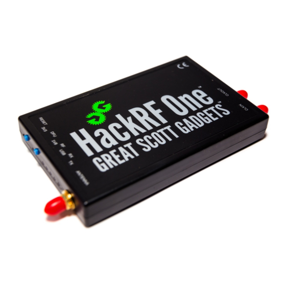
Page 15: Hackrf One
1 MHz to 6 GHz. Designed to enable test and development of modern and next generation radio technologies, HackRF One is an open source hardware platform that can be used as a USB peripheral or programmed for stand-alone operation. -
Page 16: Enclosure Options
• RF shield footprint: An optional shield may be installed over HackRF One’s RF section. • Antenna port power: HackRF One can supply up to 50 mA at 3.3 V DC on the antenna port for compatibility with powered antennas and other low power amplifiers. -
Page 17: Transmit Power
The CLKIN port on HackRF One is a high impedance input that expects a 0 V to 3 V square wave at 10 MHz. Do not exceed 3.3 V or drop below 0 V on this input. Do not connect a clock signal at a frequency other than 10 MHz (unless you modify the firmware to support this). -
Page 18: Hardware Documentation
4.10 Expansion Interface The HackRF One expansion interface consists of headers P9, P20, P22, and P28. These four headers are installed on the commercial HackRF One from Great Scott Gadgets. 4.10.1 P9 Baseband A direct analog interface to the high speed dual ADC and dual DAC. - Page 19 HackRF 4.10.2 P20 GPIO Providing access to GPIO, ADC, RTC, and power. Function VBAT RTC_ALARM WAKEUP GPIO3_8 GPIO3_0 GPIO3_10 GPIO3_11 GPIO3_12 GPIO3_13 GPIO3_14 GPIO3_15 ADC0_6 ADC0_2 VBUSCTRL ADC0_5 ADC0_0 VBUS 4.10.3 P22 I2S I2S, SPI, I2C, UART, GPIO, and clocks.
- Page 20 HackRF Function CLKOUT CLKIN RESET I2C1_SCL I2C1_SDA SPIFI_MISO SPIFI_SCK SPIFI_MOSI I2S0_RX_SCK I2S_RX_SDA I2S0_RX_MCLK I2S0_RX_WS I2S0_TX_SCK I2S0_TX_MCLK U0_RXD U0_TXD P2_9 P2_13 P2_8 CLK6 4.10.4 P28 SD SDIO, GPIO, clocks, and CPLD. Chapter 4. HackRF One...
- Page 21 HackRF Function SD_CD SD_DAT3 SD_DAT2 SD_DAT1 SD_DAT0 SD_VOLT0 SD_CMD SD_POW SD_CLK GCK2 GCK1 B1AUX14 B1AUX13 CPLD_TCK BANK2F3M2 CPLD_TDI BANK2F3M6 BANK2F3M12 BANK2F3M4 Additional unpopulated headers and test points are available for test and development, but they may be incompatible with some enclosure or expansion options.
- Page 22 HackRF Chapter 4. HackRF One...
-
Page 23: Opera Cake
CHAPTER FIVE OPERA CAKE Opera Cake is an antenna switching add on board for HackRF. 5.1 Using Opera Cake 5.1.1 Board Address As communication with Opera Cake is based on I2C, each board has an address. The default address is 24, but this can be changed by setting jumpers on P1. -
Page 24: Opera Glasses
5.2 Opera Glasses As no other software is opera cake aware, it is possible to pre-configure HackRF to support frequency bands and have opera cake automatically switch antenna when the radio retunes. The bands are specified in priority order, the final band specified will be used for frequencies not covered by the other bands specified. -
Page 25: Updating Firmware
When writing a firmware image to SPI flash, be sure to select firmware with a filename ending in “.bin”. After writing the firmware to SPI flash, you may need to reset the HackRF device by pressing the RESET button or by unplugging it and plugging it back in. -
Page 26: Only If Necessary: Dfu Boot
USB, and then execute that code from RAM. The SPIFI is normally unused and unaltered in DFU mode. To start up HackRF One in DFU mode, hold down the DFU button while powering it on or while pressing and releasing the RESET button. - Page 27 HackRF (continued from previous page) make sudo make install Now you will have the current version of DFU Util installed on your system. 6.5. Obtaining DFU-Util...
- Page 28 HackRF Chapter 6. Updating Firmware...
-
Page 29: Faq
A normal user under Linux doesn’t have the permissions to access arbitrary USB devices because of security reasons. The first solution would be to run every command which tries to access the HackRF as root which is not recommended for daily usage, but at least shows you if your HackRF really works. - Page 30 HackRF module. Use the command dmesg to check the last system log entries. If you try to start hackrf_info it will terminate with the error message and the system log will show a message like: •...
-
Page 31: Hackrf_Set_Sample_Rate Fails
7.3 What is the big spike in the center of my received spectrum? Question: I see a large spike in the center of my FFT display regardless of the frequency my HackRF is tuned to. Is there something wrong with my HackRF? Answer: You are seeing a DC offset (or component or bias). -
Page 32: How Do I Deal With The Dc Offset
0 Hz (many do), you can shift the frequency in the digital domain, moving your signal of interest to 0 Hz and your DC offset away from 0 Hz. HackRF’s high maximum sampling rate can be a big help as it allows you to use offset tuning even for relatively wideband signals. -
Page 33: System Requirements
Question: What are the minimum system requirements for using HackRF? Answer: The most important requirement is that you supply 500 mA at 5 V DC to your HackRF via the USB port. If your host computer has difficulty meeting this requirement, you may need to use a powered USB hub. -
Page 34: What Is The Receive Sensibility Of Hackrf
If you were to try to redesign the RF section on HackRF One to support full-duplex, the main thing to focus on would be the MAX2837 (intermediate frequency transceiver). This part is half-duplex, so you would either need two of them or you would have to redesign the RF section to use something other than the MAX2837, likely resulting in a radically different design. -
Page 35: Hackrf Hacks
CHAPTER EIGHT HACKRF HACKS Have you done something cool with HackRF? Let us know and we will post a link here! • Jawbreaker/VFD spectrum analyzer (Jared Boone), see also the extended demo on Hak5 • wireless microphones (Jared Boone) •... - Page 36 HackRF Chapter 8. HackRF Hacks...
-
Page 37: Getting Help
CHAPTER NINE GETTING HELP Before asking for help with HackRF, check to see if your question is listed in the or has already been answered in GitHub issues or the mailing list archives. For assistance with HackRF use or development, please look at the issues on the GitHub project. - Page 38 HackRF Chapter 9. Getting Help...
-
Page 39: Tips And Tricks
2. Use a short USB cable. Trying anything larger than a 6ft cable may yield poor results. The longer the cable, the more loss you can expect and when making this post a 15ft cable was tried and the result was the HackRF would only power up half way. - Page 40 HackRF At 8MHz sampling rate, and using the minimum 1.75MHz bandwidth filter, this is the response: You can see that the attenuation is more than 60dB at +/-2.8MHz, which is more than sufficient to remove significant adjacent spectrum interference before the ADC digitizes the baseband. If using this configuration to get a 2MHz sampling rate, use a GNU Radio block after the 8MHz source that performs a 4:1 decimation with a decently sharp low pass filter (complex filter with a cut-off of <1MHz).
-
Page 41: Firmware Development Setup
CHAPTER ELEVEN FIRMWARE DEVELOPMENT SETUP Firmware build instructions are included in the repository under firmware/README: https://github.com/mossmann/hackrf/blob/master/firmware/README... - Page 42 HackRF Chapter 11. Firmware Development Setup...
-
Page 43: Lpc43Xx Debugging
Probe had some bugs when trying to work with the M0 the last time I tried it. 12.2 LPC-Link (included with LPCXpresso boards) TitanMKD has had some success. See the tutorial in hackrf/doc/LPCXPresso_Flash_Debug_Tutorial.pdf or .odt (PDF and OpenOffice document) Doc Link [https://github.com/mossmann/hackrf/tree/master/doc) 12.3 ST-LINK/V2 12.3.1 Hardware Configuration... - Page 44 HackRF 12.3.2 Software Configuration I’m using libusb-1.0.9. Install OpenOCD-0.6.0 dev # Cloned at hash a21affa42906f55311ec047782a427fcbcb98994 git clone git://openocd.git.sourceforge.net/gitroot/openocd/openocd openocd ./bootstrap ./configure --enable-stlink --enable-buspirate --enable-jlink --enable-maintainer-mode make sudo make install OpenOCD configuration files openocd.cfg #debug_level 3 source [find interface/stlink-v2.cfg] source ./lpc4350.cfg lpc4350.cfg...
-
Page 45: Run Arm Gdb
HackRF (continued from previous page) <reg name="r7" bitsize="32" type="uint32"/> <reg name="r8" bitsize="32" type="uint32"/> <reg name="r9" bitsize="32" type="uint32"/> <reg name="r10" bitsize="32" type="uint32"/> <reg name="r11" bitsize="32" type="uint32"/> <reg name="r12" bitsize="32" type="uint32"/> <reg name="sp" bitsize="32" type="data_ptr"/> <reg name="lr" bitsize="32"/> <reg name="pc" bitsize="32" type="code_ptr"/>... - Page 46 HackRF (continued from previous page) # execution. display/32xh buffer # Print the contents of a range of registers (in this case the # CGU peripheral, starting at 0x40050014, for 46 words): x/46 0x40050014 And still more, for debugging ARM Cortex-M4 Hard Faults:...
-
Page 47: Lpc43Xx Sgpio Configuration
SGPIO is a peripheral that has a bunch of 32-bit shift registers. These shift registers can be configured to act as a parallel interface of different widths. For HackRF, we configure the SGPIO to transfer eight bits at a time. The SGPIO interface can also accept an external clock, which we use to synchronize transfers with the sample clock. - Page 48 I’d really love to be wrong about all this, but all my testing has indicated there’s no workable solution to using GPDMA that’s any better than using SGPIO interrupts to transfer samples. If you want some sample GPDMA code to experiment with, please contact Jared (sharebrained on #hackrf in Discord or IRC). Chapter 13. LPC43xx SGPIO Configuration...
-
Page 49: Lpc43Xx Usb Dfu Notes
CHAPTER FOURTEEN LPC43XX USB DFU NOTES The LPC43xx contains USB DFU bootloader support in ROM. By selecting the appropriate boot mode (USB0), the device will come up on USB at power-up or reset, and implement the popular and well-documented USB DFU protocol. -
Page 50: Jellybean Notes
HackRF echo "0000000: da ff {blocksL} {blocksH} {hash0} {hash1} {hash2} {hash3}" | xxd -g1 -r >␣ header.bin where {blocksL} and {blocksH} are the low and high bytes of the length of the .bin file + 16 bytes, measured in 512-byte frames. -
Page 51: Lpc43Xx Usb Implementation
CHAPTER FIFTEEN LPC43XX USB IMPLEMENTATION The NXP LPC43xx has a fairly sophisticated USB peripheral. It can transmit and receive chains of large buffers (by microcontroller standards), completely independently of the processor. This is excellent, as we’ll want to reserve the processor’s computational power for doing interesting things with the data. - Page 52 HackRF Chapter 15. LPC43xx USB Implementation...
-
Page 53: Hardware Components
CHAPTER SIXTEEN HARDWARE COMPONENTS Major parts used in HackRF One: • MAX2837 2.3 to 2.7 GHz transceiver Datasheet – – There’s also a register map document that Mike received directly from Maxim. Send an email to Mike or submit a support request to Maxim if you want a copy. -
Page 54: Block Diagrams
HackRF 16.1 Block Diagrams Chapter 16. Hardware Components... - Page 55 HackRF 16.1. Block Diagrams...
- Page 56 HackRF Chapter 16. Hardware Components...
-
Page 57: Clocking
SEVENTEEN CLOCKING HackRF clock signals are generated by the Si5351. The plan so far: • crystal frequency: 25 MHz (supports 25 or 27 MHz) • optional clock input frequency: 10 MHz recommended (supports 10 to 40 MHz, or higher with division) •... - Page 58 HackRF Chapter 17. Clocking...
-
Page 59: Multiple Device Hardware Level Synchronization
You will also be electrically connecting them together. If you do this incorrectly, there is a good chance one or all of the devices will be permanently destroyed. 18.2 Related work "bardi_" on the #hackrf channel pointed out his paper on synchronising HackRFs. This uses the HackRF CPLD to synchronise multiple devices. 18.3 Requirements For this to work you will need: •... -
Page 60: Opening Your Hackrf
Choose a primary HackRF, and connect the clock sync cable from the clock out connector to the clock in connector of the second HackRF. If you’re using another HackRF, connect the second HackRF’s clock out to the third HackRF’s clock in. -
Page 61: Identify The Pin Headers
The hackrf has four pin headers, three of which are arranged in a ‘C’ shape. On the board these are marked as P28, P22 and P20. - Page 62 HackRF Chapter 18. Multiple device hardware level synchronization...
-
Page 63: Wire Up The Pin Headers
P20 are GND pins. We use P20-PIN19 on both devices and connect them together like so: We then need a positive (+5v) connection to ‘fake’ the third hackrf if it’s not present. We use P20-PIN3 from the primary hackrf for this, and bring it down to the breadboard. primary:P20-PIN8 and secondary:P20-PIN8 are ready input GPIO pins for the missing third HackRF. - Page 64 HackRF Next we connect the primary:P20-PIN7 ready GPIO pin input to the secondary:P20-PIN5 ready GPIO pin output, and the primary:P20-PIN5 ack GPIO pin output to the secondary:P20-PIN7 ack GPIO pin input. This is the final step, and should look as follows:...
-
Page 65: Upgrade
The latest version of hackrf_transfer includes the ‘-H’ flag, which will activate hardware synchronisation (via libhackrf via the firmware). Testing this way is a little tricky because neither HackRF will start sending data until they are synched, and hackrf_transfer will time out if it hasn’t received any data within one second. So the test requires that two copies of _hackrf_transfer are started within 1 second of each other. -
Page 66: What Next
HackRF Run the following command: • hackrf_transfer -d <device A> -r <filename-A> -H &; hackrf_transfer -d <device B> -r <filename-B> -H If the test runs correctly, you have successfully streamed synchronised data from two HackRFs! The two streams can be merged into one using GnuRadio, and then viewed using this hacky piece of PyQt. - Page 67 HackRF 18.10. What next?
- Page 68 HackRF Chapter 18. Multiple device hardware level synchronization...
-
Page 69: Software Support
19.1 Software with HackRF Support This is intended to be a list of software known to work with the HackRF. There are three sections, GNU Radio Based software, those that have support directly, and those that can work with data from the HackRF. -
Page 70: Hackrf Tools
19.5 HackRF Tools In addition to third party tools that support HackRF, we provide some commandline tools for interacting with HackRF. For information on how to use each tool look at the help information provided (e.g. hackrf_transfer -h) or the manual pages. -
Page 71: Libhackrf Api
HackRF hardware. If you are writing a generic SDR application, i.e. not tied to the HackRF hardware, we strongly recommend that you use either gr-osmosdr or SoapySDR to provide support for the broadest possible range of software defined radio hardware. - Page 72 20.1.8 HackRF Exit Cleanly shutdown libHackRF and the underlying USB context. This does not stop in progress transfers or close the HackRF hardware. hackrf_close() should be called before this to cleanly close the connection to the hardware. Syntax: int hackrf_exit() Returns: A value from the hackrf_error constants listed below.
-
Page 73: Using The Radio
Returns: A value from the hackrf_error constants listed below. 20.2.4 HackRF Stop Tx Syntax: int hackrf_stop_tx(hackrf_device*) Params: Returns: A value from the hackrf_error constants listed below. 20.2.5 HackRF Set Baseband Filter Bandwidth Syntax: int hackrf_set_baseband_filter_bandwidth(hackrf_device*, const uint32_t bandwidth_hz) Params: Returns: A value from the hackrf_error constants listed below. -
Page 74: Reading And Writing Registers
HackRF 20.2.7 HackRF Compute Baseband Filter BW Round Down LT Compute nearest freq for bw filter (manual filter) Syntax: uint32_t hackrf_compute_baseband_filter_bw_round_down_lt(const uint32_t bandwidth_hz) Params: Returns: A valid baseband filter width available from the Maxim MAX2837 frontend used by the radio. -
Page 75: Updating Firmware
HackRF 20.3.4 HackRF Si5351C Write Write register values to the Si5351C clock generator IC. Syntax: int hackrf_si5351c_write(hackrf_device* device, uint16_t register_number, uint16_t value) Params: Returns: 20.3.5 HackRF RFFC5071 Read Read register values from the RFFC5071 mixer IC. Syntax: int hackrf_rffc5071_read(hackrf_device* device, uint8_t register_number, uint16_t*... -
Page 76: Board Identifiers
HackRF 20.4.2 HackRF SPI Flash Erase Syntax: int hackrf_spiflash_erase(hackrf_device* device) Params: Returns: 20.4.3 HackRF SPI Flash Write Syntax: int hackrf_spiflash_write(hackrf_device* device, const uint32_t address, const uint16_t length, unsigned char* const data) Params: Returns: 20.4.4 HackRF SPI Flash Read Syntax: int hackrf_spiflash_read(hackrf_device* device, const uint32_t address, const... -
Page 77: Miscellaneous
HackRF 20.5.3 HackRF Board Part ID Serial Number Read Syntax: int hackrf_board_partid_serialno_read(hackrf_device* device, read_partid_serialno_t* read_partid_serialno) Params: Returns: 20.6 Miscellaneous 20.6.1 HackRF Error Name Syntax: const char* hackrf_error_name(enum hackrf_error errcode) Params: Returns: 20.6.2 HackRF Board ID Name Syntax: const char* hackrf_board_id_name(enum hackrf_board_id board_id) -
Page 78: Enumerations
50MHz - 4GHz 20MHz Unknown Jellybean 20MHz Most boards will identify as HackRF One, Jawbreaker or Rad1o. Jellybean was a pre-production revision of HackRF. No hardware device should intentionally report itself with an invalid board ID. enum hackrf_board_id BOARD_ID_JELLYBEAN BOARD_ID_JAWBREAKER... - Page 79 0xFFFF, 20.8.3 Transceiver Mode HackRF can operate in three main transceiver modes, Receive, Transmit and Signal Source. There is also a CPLD update mode which is used to write firmware images to the CPLD. The transceiver mode can be changed with hackrf_set_transceiver_mode with the value parameter set to one of...
- Page 80 HackRF Chapter 20. libhackRF API...
-
Page 81: Jawbreaker
CHAPTER TWENTYONE JAWBREAKER HackRF Jawbreaker is the beta test hardware platform for the HackRF project. 21.1 Features • half-duplex transceiver • operating freq: 30 MHz to 6 GHz • supported sample rates: 8 Msps to 20 Msps (quadrature) • resolution: 8 bits •... -
Page 82: Sma, Not Rp-Sma
HackRF If you want to restore the PCB antenna for some reason, you can install a 10 nF capacitor or a 0 ohm resistor on the R44 pads or you may be able to simply create a solder bridge. 21.3 SMA, not RP-SMA Some connectors that appear to be SMA are actually RP-SMA. - Page 83 HackRF Selection USART0 SPIFI USB0 USSP0 USART3 P19 SPIFI Intercept header Traces may be cut to install header and jumpers or use off-board SPI flash. Function Flash DO SPIFI_MISO Flash DI SPIFI_MOSI Flash CLK SPIFI_SCK Flash CS SPIFI_CS Flash Hold...
- Page 84 HackRF P21 Analog Function ADC0_6 ADC0_2 ADC0_5 ADC0_0 P22 I2S Function I2S0_TX_SDA I2S0_TX_WS I2S0_TX_SCK I2S0_TX_MCLK P25 LPC_ISP Function U0_RXD U0_TXD RESET P26 LPC_JTAG Function RESET Chapter 21. Jawbreaker...
- Page 85 HackRF P28 SD Function SD_CD SD_DAT3 SD_DAT2 SD_DAT1 SD_DAT0 SD_VOLT0 SD_CMD SD_POW SD_CLK 21.6.2 CPLD P29 CPLD_JTAG Function CPLD_TMS CPLD_TDI CPLD_TDO CPLD_TCK P30 BANK2_AUX Function B2AUX1 B2AUX2 B2AUX3 B2AUX4 B2AUX5 B2AUX6 B2AUX7 B2AUX8 B2AUX9 B2AUX10 B2AUX11 B2AUX12 B2AUX13 B2AUX14 B2AUX15 B2AUX16 21.6.
- Page 86 HackRF P31 BANK1_AUX Function B1AUX9 B1AUX10 B1AUX11 B1AUX12 B1AUX13 B1AUX14 B1AUX15 B1AUX16 21.6.3 External clock P2 CLKOUT Install C165 and R92 as necessary to match output. For CMOS output, install 0 ohm resistor in place of C165; do not install R92.
- Page 87 HackRF P17 CLKIN_JMP Cut P17 short (trace) to enable external clock input. If short is cut, a jumper should be used on P17 at all times when an external clock is not connected to P16. Function CLKIN 21.6.4 More Additional headers are available. See the board files for additional details.
- Page 88 HackRF Chapter 21. Jawbreaker...
-
Page 89: Design Goals
TWENTYTWO DESIGN GOALS Eventually, the HackRF project may result in multiple hardware designs, but the initial goal is to build a single wideband transceiver peripheral that can be attached to a general purpose computer for software radio functions. Primary goals: •... - Page 90 HackRF Chapter 22. Design Goals...
-
Page 91: Future Hardware Modifications
CHAPTER TWENTYTHREE FUTURE HARDWARE MODIFICATIONS Things to consider for post-Jawbreaker hardware designs: 23.1 Antenna The PCB antenna on Jawbreaker was included to facilitate beta testing. Future designs likely will not include a PCB antenna. SMA connectors will be PCB edge-mounted. 23.2 Baseband The interfaces between the MAX2837 and MAX5864 have some signals inverted. -
Page 92: Usb
HackRF 23.5 USB Would support for host mode on the second USB PHY be useful somehow? This is only possible with a larger LPC43xx package that exposes the second PHY’s ULPI signals. Unless, of course, a mere full-speed PHY is acceptable. -
Page 93: Shield Support
VBAT to a shield for battery backup (disconnecting it from VCC) or providing a coin cell footprint on the HackRF PCB. Coalesce separate headers into fewer, larger banks of headers, to reduce the number of unique, small header receptacles required for mating? Reducing the header count will also increase the amount of board space around the perimeter of a shield for components and connectors. - Page 94 HackRF Chapter 23. Future Hardware Modifications...
-
Page 95: Lemondrop Bring Up
CHAPTER TWENTYFOUR LEMONDROP BRING UP Board draws approximately 24mA from +3V3 when power is applied. This seems a bit high, but may be expected if not all parts are capable of low-power mode, or aren’t configured for low power at power-on. I need to review the schematic and datasheets and see what can be done. - Page 96 HackRF (continued from previous page) Searching I2C address space. Found devices at: 0xC0(0x60 0xC1(0x60 I2C A0 address configuration pin (not available on QFN20 package) is apparently forced to “0”. 24.1.3 Reading registers # Read register 0 I2C>[0xc0 0[0xc1 # Register 0: SYS_INIT=0, LOL_B=0, LOL_A=0, LOS=1, REVID=0...
- Page 97 HackRF (continued from previous page) # CLKIN_DIV=0 (Divide by 1) # PLLB_SRC=0 (XTAL input) # PLLA_SRC=0 (XTAL input) [0xC0 0x00] # Registers 16 through 23: CLKx Control # CLK0: CLK0_PDN=0 (powered up) MS0_INT=1 (integer mode) MS0_SRC=0 (PLLA as source for MultiSynth 0)
- Page 98 HackRF (continued from previous page) MS1_P1[15: (register 53) = 0x12 MS1_P1[ (register 54) = 0x00 MS1_P2[19:0] MS1_P3[19:0] Initialization: # Disable all CLKx outputs. [0xC0 0xFF] # Turn off OEB pin control for all CLKx [0xC0 0xFF] # Power down all CLKx...
- Page 99 HackRF (continued from previous page) CLK1_PDN=0 (powered up) MS1_INT=1 (integer mode) MS1_SRC=0 (PLLA as source for MultiSynth 1) CLK1_INV=0 (not inverted) CLK1_SRC=3 (MS1 as input source) CLK1_IDRV=3 (8mA) [0xC0 0x4F 0x4F 0x80 0x80 0x80 0x80 0x80 0x80] # Enable CLK0 output only.
- Page 100 HackRF Chapter 24. Lemondrop Bring Up...
-
Page 101: Lpc4350 Sgpio Experimentation
LPCWare repository. All source I’ve found so far is focused on generating many I2S interfaces, which is not very similar to HackRF’s needs. But reviewing the code is still valuable in grasping how the SGPIO peripheral operates. There are a few common details to setting up the SGPIO peripheral: // Configure the PLL to generate a reasonable clock. - Page 102 HackRF 25.1.1 Jiggle SGPIO Pins From GPIO Mode My first test was to ensure I had the right pin(s) hooked up to my scope: // Jiggle one of the SGPIO pins in GPIO mode, to make sure // I'm looking at the right pin on the scope.
- Page 103 HackRF (continued from previous page) // Enable SGPIO pin outputs. LPC_SGPIO->GPIO_OENREG << // SGPIO12 << // SGPIO0 // SGPIO pin 0 outputs slice A bit 0. LPC_SGPIO->OUT_MUX_CFG[0] << // P_OE_CFG = X << // P_OUT_CFG = 0, dout_doutm1 (1-bit mode) // SGPIO pin 12 outputs slice D bit 0.
- Page 104 HackRF (continued from previous page) LPC_SGPIO->SLICE_MUX_CFG[3] << // INV_QUALIFIER = 0 (use normal qualifier) << // PARALLEL_MODE = 0 (shift 1 bit per clock) << // DATA_CAPTURE_MODE = 0 (detect rising edge) << // INV_OUT_CLK = 0 (normal clock) <<...
Need help?
Do you have a question about the HackRF and is the answer not in the manual?
Questions and answers