
Related Manuals for Nokia NSB-6 Series


Summary of Contents for Nokia NSB-6 Series
- Page 1 PAMS Technical Documentation NSB–6 Series Transceivers Disassembly & Troubleshooting Instructions E Nokia Mobile Phones Ltd. Issue 1 06/2000...
-
Page 2: Table Of Contents
Picture 2. RX I/Q before AGC ......E Nokia Mobile Phones Ltd. Page 2 Issue 1 06/2000... - Page 3 ....Picture 10. Clock signals, VCTCXO, RFC ... . . E Nokia Mobile Phones Ltd. Page 3 Issue 1 06/2000...
-
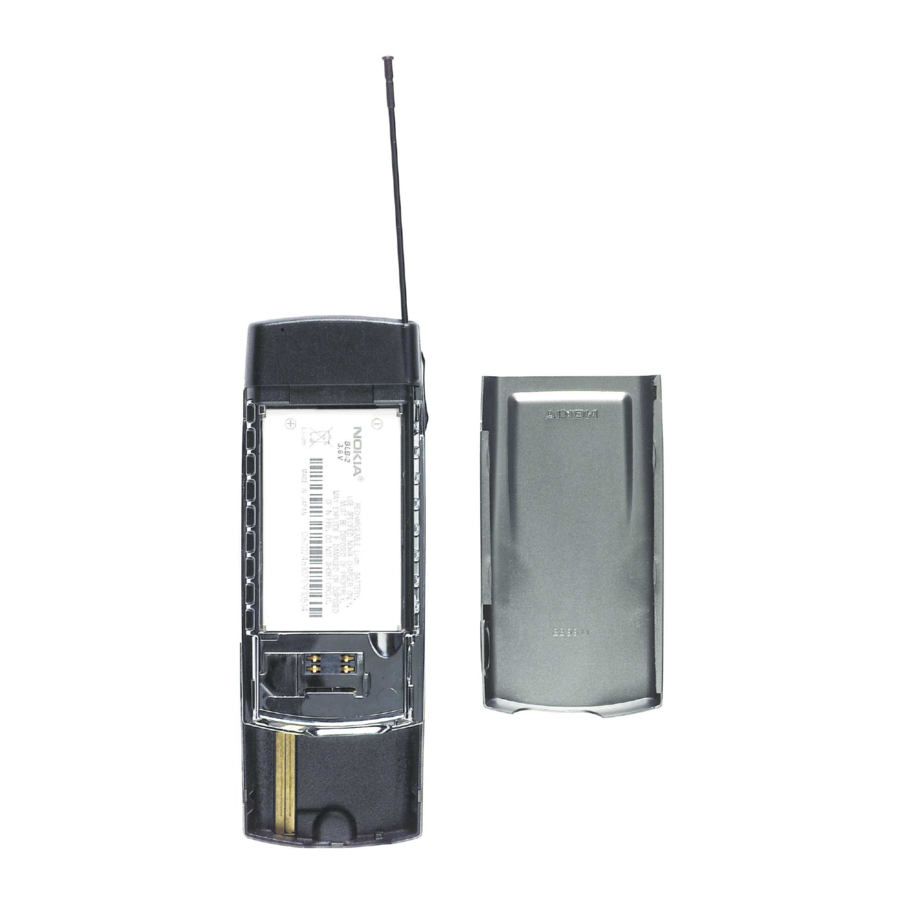
Page 4: Disassembly Of Nsb-6
Step 2. Push the slide edge outwards. NOTE: Use only numbered side 2 to release the slide. Step 3. Lift the slide up simultaneously and the slide will be released. E Nokia Mobile Phones Ltd. Page 4 Issue 1 06/2000... - Page 5 NOTE: When assembling the Remove A–cover, speaker screws, use 15 and power button. Ncm torque. Remove keymat module screws (2 pcs). NOTE: When assembling the screws, use 17 Ncm torque. E Nokia Mobile Phones Ltd. Page 5 Issue 1 06/2000...
- Page 6 SW/slide switch on the PCB. Parts can be separated: – lcd module – PCB – buzzer rubber – metal gasket – bottom connector – SIM connector – Twin Rip – vibra E Nokia Mobile Phones Ltd. Page 6 Issue 1 06/2000...
- Page 7 Remove the volume key 2. Turn the phone around. Press down battery conector springs Release the latch snap. using Battery Connector Extractor Tool. Remove the latch and latch spring. Battery connector will be released. E Nokia Mobile Phones Ltd. Page 7 Issue 1 06/2000...
-
Page 8: Transceiver Troubleshooting
MAD (D200) –> COMBO MEMORY (D210) J237 SYNTHDATA HAGAR (N505) SERIAL DATA (SDATA) MAD (D200) –> HAGAR (N505) J239 DSPXF NOT CONNECTED J240 MCURDX MCU READ MAD (D200) –> COMBO MEMORY (D210) E Nokia Mobile Phones Ltd. Page 8 Issue 1 06/2000... - Page 9 VIBRA DRIVE UI–SWITCH (N310) –> VIBRA (M300) N310 PIN 19 VIBRA VIBRA CONTROL PWM MAD (D200) –> UI–SWITCH (N310) N310 PIN 3 BUZZER BUZZER CONTROL PWM MAD (D200) –> UI–SWITCH (N310) E Nokia Mobile Phones Ltd. Page 9 Issue 1 06/2000...
- Page 10 HAGAR (N505) CHIP SELECT MAD (D200) –> HAGAR (N505) R211 FLASH PROGRAMMING VOLTAGE N220 –> COMPOMEMORY (D210) R277 ACCESSORY DETECTION XMICP –> CCONT (N100) *Not in NSB–6. #Only in NSB–6. E Nokia Mobile Phones Ltd. Page 10 Issue 1 06/2000...
-
Page 11: Pcb Test Point Pictures
NSB–6 PAMS Technical Documentation Disassembly & Troubleshooting Instructions PCB Test Point Pictures C213, RFC in normal operation J227, PURX (levels) E Nokia Mobile Phones Ltd. Page 11 Issue 1 06/2000... -
Page 12: J228, Sleepclk
NSB–6 PAMS Technical Documentation Disassembly & Troubleshooting Instructions J228, SLEEPCLK J236, RAMSELX E Nokia Mobile Phones Ltd. Page 12 Issue 1 06/2000... -
Page 13: J237, Synthdata
NSB–6 PAMS Technical Documentation Disassembly & Troubleshooting Instructions J237, SYNTHDATA J241, MCUWRX E Nokia Mobile Phones Ltd. Page 13 Issue 1 06/2000... -
Page 14: J242, Mcuad1
NSB–6 PAMS Technical Documentation Disassembly & Troubleshooting Instructions J242, MCUAD1 J245, SCLK E Nokia Mobile Phones Ltd. Page 14 Issue 1 06/2000... -
Page 15: J245, Sclk (Different Time Scale In Oscilloscope)
NSB–6 PAMS Technical Documentation Disassembly & Troubleshooting Instructions J245, SCLK (DIFFERENT TIME SCALE IN OSCILLOSCOPE) J250, COBBA (CSX) E Nokia Mobile Phones Ltd. Page 15 Issue 1 06/2000... -
Page 16: J251, Cobba(Sda)
NSB–6 PAMS Technical Documentation Disassembly & Troubleshooting Instructions J251, COBBA(SDA) J252, COBBA(CLK) E Nokia Mobile Phones Ltd. Page 16 Issue 1 06/2000... -
Page 17: J253, Pcmrxdata, Audiotest, Loop On, Input/Output Internal
NSB–6 PAMS Technical Documentation Disassembly & Troubleshooting Instructions J253, PCMRXDATA, WinTesla Audiotest, Loop ON, Input and Output Internal J254, PCMDCLK E Nokia Mobile Phones Ltd. Page 17 Issue 1 06/2000... -
Page 18: J255, Pcmsclk
NSB–6 PAMS Technical Documentation Disassembly & Troubleshooting Instructions J255, PCMSCLK J256, PCMTXDATA, WinTesla Audiotest, Loop ON, Input and Output Internal E Nokia Mobile Phones Ltd. Page 18 Issue 1 06/2000... -
Page 19: J260, Extmcuda0
NSB–6 PAMS Technical Documentation Disassembly & Troubleshooting Instructions J260, EXTMCUDA0 J299, TXP, WinTesla RF Control, TX, Burst, Tx level 14, Data Type Cont E Nokia Mobile Phones Ltd. Page 19 Issue 1 06/2000... -
Page 20: L200, Mic, No Mic Connected
NSB–6 PAMS Technical Documentation Disassembly & Troubleshooting Instructions L200, MIC, no mic connected N310 PIN 19, Vibra, activated from keypad E Nokia Mobile Phones Ltd. Page 20 Issue 1 06/2000... -
Page 21: N310 Pin 6, Buzzer_Ctrl
NSB–6 PAMS Technical Documentation Disassembly & Troubleshooting Instructions N310 PIN 6, BUZZER_CTRL R206, SENA E Nokia Mobile Phones Ltd. Page 21 Issue 1 06/2000... -
Page 22: R211, Vpp, Wintesla Self Test, Mcu Eeprom Interface
A/D reading is also zero. Now the slope is known and A/D readings can be calibrated. Calibration is included in VBATT A/D reading task. E Nokia Mobile Phones Ltd. Page 22 Issue 1 06/2000... -
Page 23: Troubleshooting
– solder joints are OK Before changing anything ALL SUPPLY VOLTAGES AND SYSTEM CLOCK / SLEEP CLOCK should be checked. Clock signal 26MHz VCXO buffer G830 V800++ 13MHz HAGAR N505 C213 E Nokia Mobile Phones Ltd. Page 23 Issue 1 06/2000... -
Page 24: System Clock
Check the signal from the RF side Change the Hagar oskilator VCXO G830 output fron N505 C833. There should be 26MHz signal. IF THERE ISN’T Change the VCXO G830 System clock picture. E Nokia Mobile Phones Ltd. Page 24 Issue 1 06/2000... -
Page 25: Sleep Clock
Layout picture B signal Clk 32kHz, should be like in SLEEP CLOCK picture. IF NOT Check R100, R154, R102, C102, C101, C113 and B100 IF OK Change the CCONT N100 Sleep clock picture. E Nokia Mobile Phones Ltd. Page 25 Issue 1 06/2000... -
Page 26: Power Supplies
PAMS Technical Documentation Disassembly & Troubleshooting Instructions Power Supplies Measure power supplies. Test points are shown in layout picture A. Layout example shown here is NSM–2. Vbat Vcore Vsyn2 Vsyn1 Vcobba Vref E Nokia Mobile Phones Ltd. Page 26 Issue 1 06/2000... - Page 27 Cconts digital parts keep MAD in reset by keeping PURX down for a delay of 62ms. Here is shown the start up sequence picture. Ch1 = Vbb Ch2 = VXO Ch3 = SleepClk Ch4 = PURX (see picture B) E Nokia Mobile Phones Ltd. Page 27 Issue 1 06/2000...
- Page 28 NSB–6 PAMS Technical Documentation Disassembly & Troubleshooting Instructions CLK 32 kHz PURX Ccont int. VXO Pwr ESysResetX FBUSTx MCUAd1 MCUWrX FBUSRx MBUS ROM1SelX MCURdX E Nokia Mobile Phones Ltd. Page 28 Issue 1 06/2000...
-
Page 29: Phone Is Totally Dead
MCU self tests are devided to those executed while power up (start up tests) and ones that can be executed with connected PC. The tests and included items are as follows: E Nokia Mobile Phones Ltd. Page 29 Issue 1 06/2000... - Page 30 A. Power off B. Security data C. EEPROM tune checksum D. PPM checksum E MCU download DSP F. DSP alive G. COBBA serial H COBBA parallel I. EEPROM checksum K. PPM validity E Nokia Mobile Phones Ltd. Page 30 Issue 1 06/2000...
-
Page 31: Sim Related Faults
IF NOT OK Check the Vsrm (C131 RF side head) Change the CCONT N100 V5V (C108 bottom connector side head) IF NOT OK Check the regulator N600, V116, C132 and C131 E Nokia Mobile Phones Ltd. Page 31 Issue 1 06/2000... -
Page 32: Audio Faults
Check the voltage in resistor Check R266, C268, L200 and V250 R267 RF side head. Voltage should be about 2.1V Check the R268, C263, C276 Change the COBBA N250 and C262 E Nokia Mobile Phones Ltd. Page 32 Issue 1 06/2000... - Page 33 Change the COBBA N250 Headset earphone doesn’t work and there isn’t any mechanical problem Check R 257,R256, R270, L303, L304, C303, C304, C296, C297, R218 and R219 Change the COBBA N250 E Nokia Mobile Phones Ltd. Page 33 Issue 1 06/2000...
-
Page 34: Charging Fault
Display ” not charging” Check charge voltage with wintesla Check F101, V100,R104 and R103 Check charge current calibration with WinTesla IF NOT OK Check V101 and R131 Change the Chaps N101 E Nokia Mobile Phones Ltd. Page 34 Issue 1 06/2000... -
Page 35: Rf Testpoints (Reference Pictures At The Back Of The Binder)
(32,5 dBm, EGSM / lev 5) (29,5 dBm, EGSM / lev 0) (check level from reference engine) TX14 PA output GSM C758 PA output signal TX20 PA output DCS C743 (check level from reference engine) E Nokia Mobile Phones Ltd. Page 35 Issue 1 06/2000... - Page 36 VXO3 26 MHz G830 / C833 Clock signal from VCTCXO to Hagar VXO4 13 MHz V800 / R834 RFC from Hagar to MAD Other checking points SCLK R205 SENA R206 SDATA J237 E Nokia Mobile Phones Ltd. Page 36 Issue 1 06/2000...
-
Page 37: Pictures From Rf Measurement Points
Channel 3: RX3 LNA_G V907 Note the premonitoring steps at the beginning of the burst. Picture 2. RX I/Q before AGC Pin = –50dBm, Fin = 947,06771MHz Channel 1: RX2 C522 E Nokia Mobile Phones Ltd. Page 37 Issue 1 06/2000... -
Page 38: Picture 3. Lna Control
Channel 2: TX19 C711, VPCTRL_G, (equals TX1 C714, VPCTRL_P, in upperband mode) Channel 3: TX10 C792, TXC EGSM, (equals TX10, C792, TXC DCS in upperband mode) Channel 4: TX4 C722, VtxB EGSM, (equals TX5, C752, VtxB DCS in upperband mode) E Nokia Mobile Phones Ltd. Page 38 Issue 1 06/2000... -
Page 39: Picture 5. Vbatt During Tx Burst
Channel 1: TX2, VBATT Picture 6. Switch control Channel 1: TX3: TXP, J519, Channel 2: TX10: C746, TXVGSM (equals TX16: C747, TXVDCS in upperband mode) (Channel 4: TX16: C747, TXVDCS) E Nokia Mobile Phones Ltd. Page 39 Issue 1 06/2000... -
Page 40: Picture 7. Power Detector Control
TX7: C761, DET0, Channel 2: TX6: R754, TXVDET, Channel 1: TX3: TXP, J519, Picture 8. TX IQ signals TXQN Channel 1: TX8 TXIN Channel 2: TX9 (TX burst mode Cont1) E Nokia Mobile Phones Ltd. Page 40 Issue 1 06/2000... -
Page 41: Picture 9. Vco, Operating Voltages
Channel 2: VCO1 C805, Vcc Channel 3: VCO3 N600, Vin Channel 4: VCO2 C782, Vchp Picture 10. Clock signals, VCTCXO, RFC Channel 1: VXO3 L800, RFC Channel 2: VXO4 R833, VCTCXO_out E Nokia Mobile Phones Ltd. Page 41 Issue 1 06/2000... - Page 42 NSB–6 PAMS Technical Documentation Disassembly & Troubleshooting Instructions This page intentionally left blank. E Nokia Mobile Phones Ltd. Page 42 Issue 1 06/2000...
Need help?
Do you have a question about the NSB-6 Series and is the answer not in the manual?
Questions and answers