
Summary of Contents for Diamond Systems GPIO-MM
- Page 1 GPIO-MM FPGA-based PC/104 FPGA Pinout Guide V1.01 © Copyright 2007 Diamond Systems Corporation 1255 Terra Bella Ave. Mountain View, CA 94043 Tel (650) 810-2500 Fax (650) 810-2525 www.diamondsystems.com...
- Page 2 , Y1 ..............................5 Z OSCILLATOR LED, D1................................5 TATUS XCF02S PROM, U9 ..........................5 CONFIGURATION 256- 24C04 EEPROM, U12..........................5 BYTE 74XX164 , U11............................5 SHIFT REGISTER 74XX245 , U2-U7 ............................5 BUFFERS PIN DEFINITIONS ................................6 Diamond Systems Corporation GPIO-MM FPGA Pinout Guide V1.01 Page 2...
-
Page 3: General Description
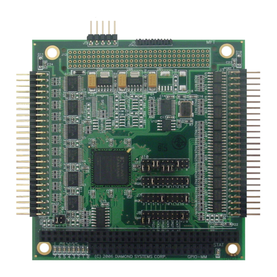
1 GENERAL DESCRIPTION The FPGA on the GPIO-MM is connected to the following devices: 1.1 PC/104 connectors J1 and J2 The FPGA connects directly to the PC/104 signals: Address bus: SA<19:0> Data bus: SD<15:0> Control lines: AEN, IOR#, IOW#, SMEMRD#, SMEMWR#, MEMRD#, MEMWR#, TC, RESET 16-bit control: IOCS16#, MEMCS16#, SBHE# IRQ and DMA signals are routed through configuration blocks J7-J9. - Page 4 +3.3V. If the jumper is present, the signal is pulled low to 0V. These inputs can be used for any kind of binary user configuration. One common use is for I/O address selection. Diamond Systems Corporation GPIO-MM FPGA Pinout Guide V1.01 Page 4...
- Page 5 B with the data on port A (i.e. use this to output data from the FPGA to J4). When the direction signal is low, the buffers drive port A with the data on port B (i.e. use this to input data from J4 to the FPGA). Diamond Systems Corporation GPIO-MM FPGA Pinout Guide V1.01 Page 5...
-
Page 6: Pin Definitions
DIO_J3_40 J3 pin 40 Digital I/O DIO_J3_41 J3 pin 41 Digital I/O DIO_J3_42 J3 pin 42 Digital I/O DIO_J3_43 J3 pin 43 Digital I/O DIO_J3_44 J3 pin 44 Digital I/O Diamond Systems Corporation GPIO-MM FPGA Pinout Guide V1.01 Page 6... - Page 7 Digital I/O DIO_J4_39 J4 pin 39 (U6) Digital I/O DIO_J4_40 J4 pin 40 (U7) Digital I/O DIO_J4_41 J4 pin 41 (U6) Digital I/O DIO_J4_42 J4 pin 42 (U7) Digital I/O Diamond Systems Corporation GPIO-MM FPGA Pinout Guide V1.01 Page 7...
- Page 8 PC/104 A19 Address Bus SA11 PC/104 A20 Address Bus SA10 PC/104 A21 Address Bus PC/104 A22 Address Bus PC/104 A23 Address Bus PC/104 A24 Address Bus PC/104 A25 Address Bus Diamond Systems Corporation GPIO-MM FPGA Pinout Guide V1.01 Page 8...
- Page 9 EEP_SDL U12 pin 5 EEPROM Data Line EEP_SCL U12 pin 6 EEPROM Clock Line 74HC164 GROUP IDCLK U11 pin 8 74HC164 Data IDDAT U11 pin 1 and 2 74HC164 Clock Diamond Systems Corporation GPIO-MM FPGA Pinout Guide V1.01 Page 9...
Need help?
Do you have a question about the GPIO-MM and is the answer not in the manual?
Questions and answers