Table of Contents
Advertisement
Contents of this brochure:The main story S9 Troubleshooting of various faults in the Operation board,how to use the test box for accurate
positioning.
Range:Applies to All S9 Production,After sale,Outside the coordination repair site
One Maintenance Platform Requirements:
1, Thermostatic soldering Irons(350 -400 ),Tip tip for solder chip resistor capacitors and other small patches.
2, hot air cylinder for chip disassembly welding,be careful not to heat up for a long time lest PCB Foaming.
3, APW3 Power(Output 12V、133A Max),Used for test measurement of the Operation board.
4. Multimeter,Sub-camera,S9 Test Jigs(Conditional configurable Oscilloscope)。
5, flux, washing plate water plus anhydrous alcohol;Wash plate water is used to clean and repair the residue and appearance of welding.
tin-Planting fixture,Tin-sik Steel mesh,Solder Paste;When replacing a new chip,you have to plant tin on the chip.
7, Thermal conductive adhesive black(3461),Re-glue the heatsink after servicing.
Two Job requirement Items:
1、 Maintenance personnel must have some knowledge of electronics,More than one year of maintenance experience,对 QFN Packaging
welding technology Proficiency.
2、 After maintenance, the operation board must be tested two times OK,before you can pass!
3、 Pay attention to the operation method when replacing the chip,after replacing any accessory PCB No obvious deformation of the
plate,Check the replacement parts and the surrounding there are few open circuit problems. 4、 Determine the maintenance station
object and the corresponding test software parameters, test fixture.
5、 Inspection Tools,Whether the fixture can work properly
Three, principle and structure:
●Principle Overview
1. S9 is composed of 21 voltage domains connected in series. There are 3 BM1387 chips in each voltage domain, and there are 63 BM1387 chips in the whole
board.
2. The BM1387 has a built-in buck diode with a step-down diode function that is determined by the chip's designated pin
3. S9 is 21 voltage domains (S5+ is 16 voltage domains, S7 54 chip is 18 voltage domains, S7 45 is 15 voltage domains); S9 clock is 25M single crystal
oscillator, connected in series by The first chip is passed to the last chip.
4. S9 There are independent small heat sinks on the front and back of each chip. The small heat sink on the front side is the SMT patch. The small heat sink on
the back side is fixed on the back of the IC by the thermal adhesive after the initial measurement. Repair and replacement chip test
After the test, you need to evenly apply black thermal adhesive on the IC surface and heat it.
It is important to note that:
In the maintenance process, in order to reduce the damage of the high temperature of the air gun to the PCB and the chip when replacing the
components of the electric board or the chip, it is necessary to first place the small heat sink near the faulty component and the PCB board.
After the small heat sink on the back is removed, replace it.
The PCB board has test points anyway, during the maintenance of the production, the front test points can be used when the heat sink is not
attached to the front of the PCB; the finished product repair (after-sales maintenance), due to the front and back of the PCB
Covered with heat sinks, it is necessary to locate the fault through the test points of the PCB. The special slender pen can be used to probe the
gap of the heat sink for measurement, but since the SMT small heat sink is connected to the ground of each voltage domain,
When measuring, pay attention to the insulation of the test leads to avoid short circuit caused by the test leads. .
Preparation Deng Yi
Advertisement
Table of Contents

Related Manuals for Antminer S9

Summary of Contents for Antminer S9
- Page 1 The first chip is passed to the last chip. 4. S9 There are independent small heat sinks on the front and back of each chip. The small heat sink on the front side is the SMT patch. The small heat sink on the back side is fixed on the back of the IC by the thermal adhesive after the initial measurement.
- Page 2 00 chip to 62 chip transfer chip transmission chip transmission; no IO signal, standby It is 0V during standby, and is calculated during operation. It is 1.8V when calculating. 2. Figure 3 shows the key circuits on the front of the S9 computing board. 1), test points between each chip(After zooming in the image below):图 2 During maintenance,the test point between the test chip is the...
- Page 3 Note that: Because the version of the S9 computing board is not exactly the same, the LDO-1.8V power supply of the early voltage domains is powered by a separate peripheral LOD power supply chip for each of the three voltage domains. The later version is changed to the internal chip. Power supply (BM1387 chip with 2.5 V input, 1.8 V output LDO supply circuit), except for the last six voltage domains, which are powered by 14V boost and LDO externally, all other chips provide LDO1.8V power...
- Page 4 Principle analysis of single chip in voltage domain(Figure 5 Figure 6 below): 5、BM1387 Circuit diagram 6、BM1387 Chip Pin Signal Description Active Name Description Level NRSTO Output to the chip of next level, for the loop Respond Busy Output RI_A Auxiliary Respond Input add diode and pulldown Respond Input.
- Page 5 Command Output CLKO Clock output to the chip of next level, for the loop. Pin drive current: 16A PLL_VSS PLL ground PLL_VDD PLL power (0.8V), PLL digital and analog share the same supply VDDIO_08 IO VDD pre-drive, 0.8v LDO_08O LDO 0.8v output, for PLL and IO pre-drive LDO_18I LDO power input voltage range: 1.62v ~ 1.98v VDDIO_18...
- Page 6 Figure below 7 is shown: The signal voltage of each chip can be measured,CORE VoltageLDO-1.8 or、LDO-1.8I、PLL-0.8、LDO-2.5I Equal voltage: CORE:0.4---When this voltage is abnormal,Generally the voltage domain of the chip CORE Short circuit LDO-1.8 or:1.8---When this voltage is abnormal,The chip LDO-1.8 or Or LDO-1.8I Short or open circuit LDO-1.8I:1.8---When this voltage is abnormal,The chip LDO-1.8 or Or LDO-1.8I Short or open circuit PLL-0.8:0.8 in---When this voltage is abnormal,the voltage domain has a chip PLL-08 Power supply short-circuit, or LDO-1.8 Abnormal.
- Page 7 S9 Operator Board Maintenance Instructions 8. IO Pin definition for each port As shown in the figure above: 1、2、9、10、13、14 :GND。 3、4 (SDA、SCL):DC-DC PIC I2C Bus,Connect the Control Panel to PIC of communication,The control board can read and write through it PIC Data,Control the operating state of its operational board.
- Page 8 S9 Operator Board Maintenance Instructions 10、IO The signal is divided into piezoelectric 4、14V Boost circuit: Responsible for the DC-DC(8.3 — 9.2 V)Boost to 14V,The principle is through U110 (RT8537) The switching power supply will boost 9v to 14 V,The switching signal produced by U110 passes the output switch signal through L1 The switching signal produced by U110 passes the output switch signal through L1 for storage.
- Page 9 Operator Board Maintenance Instructions Need to be aware of:An abnormally high voltage rise in the boost circuit can lead to the calculation board finally 6 Voltage domain. LDO Damage,also easily lead to chip damage. While the boost voltage the exception is mostly U110、R812、R811 Oxidation-induced. 5、DC-PIC:...
- Page 10 S9 Operator Board Maintenance Instructions 16、DC-DC Circuit LM27402SQ Voltage Regulator Generation PWM Switching signals drive up and down bridges (Two pairs CMOS),and through L2 Inductor Energy Storage, Again by C19、C20 Filtering. LM27402SQ Main function Pin Pin 7 :12V Power supply,...
- Page 11 SPX5205M5 pin 1, 3 as input,pin 5 for 1.8V Output; It is important to note that:S9 of the Operation board LDO There are two modes of power supply operation. One is that each voltage domain of an operational board is an external LDO ,SPX5205M5,Responsible for each voltage domain's 3 A chip.
- Page 12 Operator Board Maintenance Instructions 21, temperature sensing schematic diagram ●Quick Troubleshooting method: ○Troubleshooting the Whole Machine: 1, Login Monitoring interface(WEB)。 This type of failure is mostly caused by an operational board failure.,A few are due to the operating environment, fans, external network, firmware and so on. Here are some of the common phenomena that are handled:...
- Page 13 S9 Operator Board Maintenance Instructions 23、25M LCK Circuit Above phenomenon,The mining machine has been running. 7 days,0 GH/S( Avg)And did not fall much,The description of the mine machine is the time of failure. The speed of the double fan is very low,And the Temp Chip of the 8 chain is Very low,which is a board that's been dropped...
- Page 14 S9 Operator Board Maintenance Instructions 25, less mining machine 1 Block Operation Board Phenomenon 26, Mining machine Less board, Chip hit X Phenomenon The above phenomenon is caused by the failure of the mining machine calculation board. In Figure 23, the 8-board computing board only found 34 chips. Please use the tool to perform single-check on the 8th board to find out the cause of the fault.,...
- Page 15 S9 Operator Board Maintenance Instructions 27, Chip full dozen Xx The above phenomenon GH / S (RT) is 0, GH / S (AVG) computing power is reduced, the chip is all XX, red light flashes. Most of this phenomenon is caused by abnormal operation of the control panel after the mining machine is disturbed.
- Page 16 S9 Operator Board Maintenance Instructions 29、GH/S(avg)Low-Power chip full-dozen X Within 4 hours of operation, the HW has reached 150,000. As many as this, first test each board with a test tool. If the board test is ok, please keep the configuration updated to the most firmware.
- Page 17 S9 Operator Board Maintenance Instructions 31 No GH/S(RT)Red light Alarm Alarm phenomenon:Most are network exceptions,Temperature anomalies,Or the fan is abnormal. As you can see in the figure above,The sanbanxi temperature has exceeded Temp(chip)The upper limit and protect The alarm. In this case, please check the air volume of the Mining machine duct,Is there any blockage in the duct?Whether the fan is damaged?Whether there is dust in the tooth seam between the plate heatsink?...
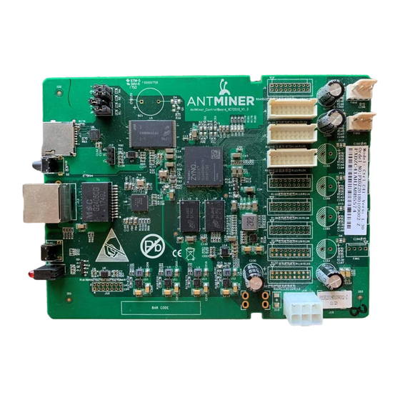
- Page 18 S9 Operator Board Maintenance Instructions 33、XILINX Control Panel However, I can't see the overall structure of the control panel during the maintenance and repair of the whole machine. We can identify the appearance of the whole machine: for example, the network indicator of the C5 control board is down, as shown in Figure 34 below; the network port of the XILINX control board is up, as shown in Figure 35 below..
- Page 19 8、 After the record.,Re-installed into the whole machine for normal testing. Fault type: S9 Common fault types are: 1、 Heat sink, heatsink shift, variant; Not allowed on the back of the board chip before powering on PCB Heatsink displacement on the board,Have collided,In particular, different voltages of the heatsink.
- Page 20 TX Signal:1.8 in;This signal is determined by the 00、01、、、、、、62 Number of chips,When the dichotomy of a point anomaly, forward detection can be. RX Signal:1.8 in;This signal is determined by the 62、、、、、、01、00 Number returned by the,Identify the cause of the fault through chip signal direction,S7 和 S9 运 The board does not run the signal as the highest priority,First find the signal.
Need help?
Do you have a question about the S9 and is the answer not in the manual?
Questions and answers