Table of Contents

Subscribe to Our Youtube Channel
Related Manuals for WinSystems PCM-MIO-A-1


Summary of Contents for WinSystems PCM-MIO-A-1
- Page 1 PCM-MIO-A-1 16 Channel, 16-bit Analog Inputs 8 Channel, 12-bit Analog Outputs, and 48 Digital I/O Product Manual WINSYSTEMS, Inc. | 2890 112th Street, Grand Prairie, Texas 75050 | 817-274-7553 | info@winsystems.com | www.winsystems.com...
- Page 2 Copyright 2020, WINSYSTEMS, Inc. No part of this document may be copied or reproduced in any form or by any means without the prior written consent of WINSYSTEMS, Inc. The information in the document is subject to change without notice. The information furnished by WINSYSTEMS, Inc.
-
Page 3: Table Of Contents
PCM-MIO-A-1 Table of Contents Before You Begin........... 5 1.1 Warnings . - Page 4 PCM-MIO-A-1 8.1.4 Multiplexer Channel Selection ......... 19 8.2 D/A Converters .
-
Page 5: Before You Begin
(including cable drawings and pinouts) that can be used with your PCM-MIO-A-1. Functionality The PCM-MIO-A-1 is a versatile, PC/104 analog input, analog output, and digital I/O board designed for high accuracy and high channel count analog and digital I/O. The board is based upon Linear Technology’s state- of-the-art precision converters and voltage references, which require no external calibration. -
Page 6: Base I/O Address
“Software Summary” on page 17. The PCM-MIO-A-1 can be configured to use IRQs 3, 4, 5, 6, 7, 9, 10, 11, 12, 14, or 15 depending on availability in the system. IRQs 0, 1, 2, 8, and 13 are not supported. -
Page 7: Features
PCM-MIO-A-1/Features Features The PCM-MIO-A-1 provides the following features. Analog Input • Two 8-channel, 16-bit analog-to-digital (A/D) (LTC-1859CG) with sam- ple-and-hold-circuit support • Conversion rate: 100 Ksps max. • Any combination of up to 16 single-ended input channels and up to 8 differential input channels •... -
Page 8: General Operation
General Operation System Block Diagram The PCM-MIO-A-1 utilizes a Lattice MachXO2 FPGA to communicate between the PC/104 ISA bus and the ADCs, DACs, and 48 DIO. The analog 16-bit inputs provide up to 100 Ksps, and ±25 V protection via the Linear Technology LTC1859 ADC converters. - Page 9 PCM-MIO-A-1/Specifications Feature Specification Environmental Temperature -40 to +85°C (-40 to +185°F) Humidity (RH) 5% to 95% non-condensing Mean time between MTBF (hours) 1074379 failure (MTBF) MTBF (years) 122.646 RoHS Compliant Operating Systems Compatible with Windows and Linux a. A MTBF measurement is based on a statistical sample and is not intended to pre- dict any one specific unit's reliability;...
-
Page 10: Configuration
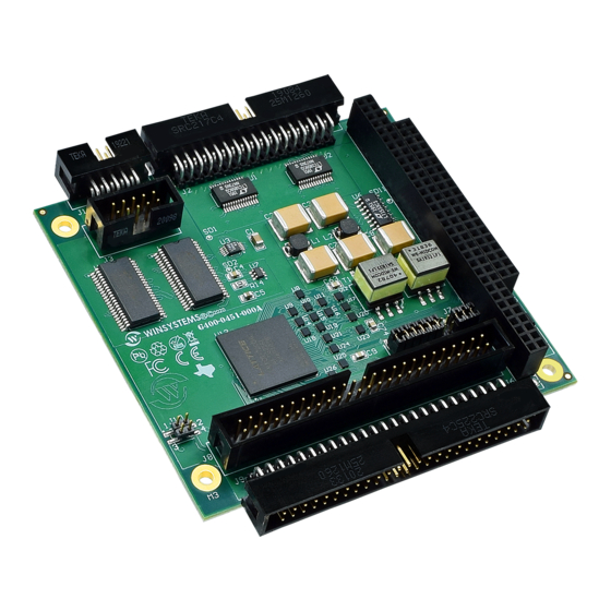
PCM-MIO-A-1/Configuration Configuration This section describes the PCM-MIO-A-1 components and configuration. Component Layout 7.1.1 Top View Analog output Analog output Digital I/O Vcc enabled Analog input Digital I/O Digital I/O PC/104 connector PC/104 connector Default base I/O address Item Description Reference... -
Page 11: Jumper Reference
NOTE Jumper part numbers W/S# G201-0002-005 and SAMTEC 2SN-BK-G are applicable to all jumpers. These are available in a five piece kit from WINSYSTEMS (Part# KIT-JMP-G-200). 7.2.1 J7 - Base I/O Address Jumpers ThePCM-MIO-A-1 is I/O mapped and requires 32 sequential port addresses. -
Page 12: J10 - Digital I/O Vcc Enable Jumpers
No power at pin 49 of J8/J9 (default) Connector Reference 7.3.1 J2 - ADC Analog Input Header The PCM-MIO-A-1 and PCM-MIO-A-AD-1 analog-to-digital conversion inputs are implemented by using two, 16-bit Linear Technology LTC- 1859CG devices. The board supports up to 16 single-ended input channels, 8 differential input channels or various combinations of both. -
Page 13: J1, J3 - D/A Analog Output Headers
7.3.2 J1, J3 - D/A Analog Output Headers NOTE The D/A converters are not available on the PCM-MIO-A-AD-1. The PCM-MIO-A-1 provides digital-to-analog conversion output using two of the 12-bit Linear Technology LTC-2704 devices. These SoftSpan quad digital-to-analog converters (DACs) are software programmable for either unipolar or bipolar mode with specific voltage ranges on a per channel basis. -
Page 14: J8, J9 Digital I/O Headers
Mating connector: ITW-PANCON 050-010-455A 7.3.3 J8, J9 Digital I/O Headers The PCM-MIO-A-1 and PCM-MIO-A-AD-1 use the Lattice MachXO2 FPGA with WINSYSTEMS WS16C48 ASIC compatible programmed logic. The 48 lines are each individually programmable as input or output and the first 24 lines are capable of fully latched event sensing with edge polarity being software programmable. - Page 15 PCM-MIO-A-1/Configuration Layout and Pin Reference Diagram Name Name Diagram Name Name Port 0 Bit 0 Port 3 Bit 0 Port 0 Bit 1 Port 3 Bit 1 Port 0 Bit 2 Port 3 Bit 2 Port 0 Bit 3 Port 3 Bit 3...
-
Page 16: J5, J6 - Pc/104 Connectors
# = Active low signal Rows C and D are not required on 8-bit modules. B10 and C19 are key locations. WINSYSTEMS uses key pins as connections to GND. Signal timing and function are as specified in ISA specification. Signal source/sink current differ from ISA values. -
Page 17: Software Summary
TEKA PC220-A-W1A7-M (J5) Software Summary A/D Converters The PCM-MIO-A-1 uses two Linear Technology LTC-1859CG 8-channel A/D converters. Each device is independently software configurable to support the listed input modes and ranges. The devices use a full-duplex serial interface which transmits and receives data simultaneously. An 8-bit command is shifted into the ADC interface to configure it for the next conversion. -
Page 18: A/D2 - Starting At Base +4
PCM-MIO-A-1/Software Summary 8.1.2 A/D2 - Starting at BASE +4 The interface for the second A/D device is almost identical to the first device. Notice in this table that the REGISTER SELECT function within the RESOURCE ENABLE register is only a single bit. In both software examples shown below, action 1 (one) should be replaced with: 1. -
Page 19: Command Register
PCM-MIO-A-1/Software Summary 8.1.3 Command Register Each A/D device contains an 8-bit command register to configure the inputs as single-ended or differential with a desired input range of 0 V–5 V, 0 V–10 V, ±5 V, and ±10 V. The following describes the register options. - Page 20 PCM-MIO-A-1/Software Summary Input Range Selection GAIN INPUT RANGE ±5 V 0 V to 5 V ±10 V 0 V to 10 V Examples of Multiplexer Options Examples of multiplexer options and changing the MUX assignment on The fly are shown below.
- Page 21 PCM-MIO-A-1/Software Summary Example 1 - ADC1 The following is a polled mode example for A/D1. 1. Write xxx00xxx to bits 3 & 4 of BASE +3. Select access to CMD 2. Write CMD selection to BASE +2. Set MUX channel operation & range 3.
-
Page 22: D/A Converters
Master Interrupt Status Register. D/A Converters The PCM-MIO-A-1 contains two Linear Technology LTC-2704 digital-to- analog converter (DAC) devices. Each device is a 4-channel converter with software selectable output span. -
Page 23: Command Register
PCM-MIO-A-1/Software Summary Address Read/ Register (Base+) Write DATA_LO LOW ORDER DATA BYTE DATA-BIT 7 DATA-BIT 6 DATA-BIT 5 DATA-BIT 4 DATA-BIT 3 DATA-BIT 2 DATA-BIT 1 DATA-BIT 0 READBACK LOW ORDER DATA BYTE DATA-BIT 7 DATA-BIT 6 DATA-BIT 5 DATA-BIT 4... -
Page 24: Command Codes
PCM-MIO-A-1/Software Summary configure the span and load the data. The command word consists of a 4 bit command and a 4-bit address, as shown. 8.2.4 Command Codes NOTE Codes not shown are reserved and should not be used. Readback Point... -
Page 25: Readback Enable
PCM-MIO-A-1/Software Summary Span Unipolar 0 V to 5 V Unipolar 0 V to 10 V Bipolar -5 V to 5 V Bipolar -10 V to 10 V Bipolar -2.5 V to 2.5 V Bipolar -2.5 V to 7.5 V 8.2.7 Readback Enable... - Page 26 PCM-MIO-A-1/Software Summary single instruction sequence. The second option is to pre-load the configuration and output data using command values 2Xh and 3Xh and then present the values to the DAC either individually (with command value 4Xh) or simultaneously (with command value 5Xh).
-
Page 27: Registers
DAC channels with a single instruction sequence. Registers 8.3.1 Register Definitions (WS16C48 Logic) The PCM-MIO-A-1 and PCM-MIO-A-AD-1 use a Lattice MachXO2 FPGA with WINSYSTEMS WS16C48 ASIC compatible programmed logic. This provides 48 lines of digital I/O. There are 17 unique registers within the WS16C48 v1.0... -
Page 28: Register Details
PCM-MIO-A-1/Software Summary logic. The following table summarizes the registers, and the text that follows provides details on each of the internal registers. BASE+ I/O Address Offset Page 0 Page 1 Page 2 Page 3 Port 0 I/O Port 1 I/O... - Page 29 PCM-MIO-A-1/Software Summary IRQ_REG This register is accessible when Page 0 is selected. It is used to select the bus routine for the generated interrupt. REV_LO This register is accessible when Page 0 is selected. This register returns the low byte of the current revision level for the FPGA firmware.
-
Page 30: Accessories
PCM-MIO-A-1/Accessories Accessories The following table lists available WINSYSTEMS accessories for the PCM- MIO-A-1. Go to www.winsystems.com for more information on WINSYSTEMS cables and batteries. Item Part Number Description Termination board ISM-TRM-RELAY Industrial PC/104 relay board, 16 SPDT relays Termination board... -
Page 31: Best Practices
PCM-MIO-A-1/Best Practices Appendix A. Best Practices The following paragraphs outline the best practices for operating the PCM-MIO-A-1 in a safe, effective manner, that does not damage the board. Read this section carefully. Power Supply Avoid Electrostatic Discharge (ESD) Only handle the circuit board and other bare electronics when electrostatic discharge (ESD) protection is in place. - Page 32 Power Supply OFF—Always turn off the power supply before connecting to the I/O Module. Do not hot-plug the PCM-MIO-A-1 on a host platform that is already powered. I/O Connections OFF—Turn off all I/O connections before connecting them to the PCM-MIO-A-1 or any other I/O cards.
- Page 33 PC/104 board has been improperly plugged onto the stack. Conformal Coating Applying conformal coating to a WINSYSTEMS product does not in itself void the product warranty, if it is properly removed prior to return. Coating can change thermal characteristics and impedes our ability to v1.0...
- Page 34 PCM-MIO-A-1/Best Practices test, diagnose, and repair products. Any coated product sent to WINSYSTEMS for repair will be returned at customer expense and no service will be performed. Operations/Product Manuals Every WINSYSTEMS product has an Operations manual or Product manual. Periodic updates—Operations/product manuals are updated often.
-
Page 35: Mechanical Drawings
PCM-MIO-A-1/Mechanical Drawings Appendix B. Mechanical Drawings The mechanical drawing for the PCM-MIO-A-1 is shown below. v1.0 www.winsystems.com Page 35... -
Page 36: Warranty Information
Customer for the purchase of Products or licensing of Software hereunder. In the event this Order is placed in the hands of an attorney or collection agency by WINSYSTEMS to collect any sums due hereunder to WINSYSTEMS, Customer shall pay all reasonable attorney's fees, expenses, collection and court costs incurred by WINSYSTEMS.
Need help?
Do you have a question about the PCM-MIO-A-1 and is the answer not in the manual?
Questions and answers