
Related Manuals for PICOLAS LDP-CWL 06-20

Summary of Contents for PICOLAS LDP-CWL 06-20
- Page 1 User Manual LDP-CWL 06-20 LDP-CWL 12-20 - Preliminary Manual - PicoLAS GmbH Burgstr. 2 52146 Würselen Germany Phone: +49 (0) 2405-64594-60 Fax: +49 (0) 2405-64594-61 E-mail: info@picolas.de Web: www.picolas.de Rev.2102...
-
Page 2: Table Of Contents
How to use this manual......................3 Dos and don’ts.......................... 4 Required laser diode pin out....................8 Laser driver block diagram ....................9 Description of the connectors of the LDP-CWL 06-20 / LDP-CWL 12-20..9 Modes and power dissipation..................13 Frequency response ......................17 Trigger delay ..........................18 Test load ............................19... -
Page 4: How To Use This Manual
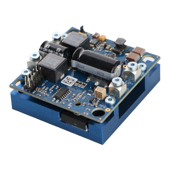
Please set the laser diode driver only in the scheduled working area and only while the power supply is turned off. Therefore please have a look at the section “Description of the Connectors of the LDP-CWL 06-20 / LDP-CWL 12-20”. Never disconnect or connect the load while the driver is operational, as it destroys the driver and/or the connected load. - Page 5 How to get started Picture 1: LDP-CWL driver with connectors, jumper and measurement points The basic settings such as output current limit setting for the crowbar can be adjusted by the Potentiometer 1. The actual adjusted maximum output current limit can be measured at MP1 (measurement point 1). An additional waveform generator might be needed which has to be connected to the input terminal.
- Page 6 Step What to do Check Connect a dummy diode between Refer to section “Test Load”. LD+ and LD-. Alternatively make a Range of compliance voltage short circuit there. 0 V .. 20 V. Set the working point of the LDP- There are three different working CWL to modulation mode (Mod.).* points: CW mode, modulation...
-
Page 7: Required Laser Diode Pin Out
Required Laser Diode Pin Out The LDP-CWL 06-20 / LDP-CWL 12-20 is designed for the direct connection of almost any kind of laser diode with a maximum compliance voltage of 20 V. The pitch of the LD- and LD+ connectors is 15.5 mm. -
Page 8: Laser Driver Block Diagram
Laser Driver Block Diagram Picture 2: Block diagram of the laser driver Description of the Connectors of the LDP-CWL 06-20 / LDP-CWL 12-20 Picture 3: Connectors of the laser driver... - Page 9 Connector Function Description Power connector: V Screw terminal M3 Power connector: GND for V Screw terminal M3 input signal Pin header See section “Connection Pin header” Jumper J1 Set the working area. See section “Modes and Power Dissipation” Laser diode connector (anode) Laser diode connector (cathode) #1 and #2.
- Page 10 #3. Connection Pin header (for LDP-CWL 12-20) Function number N.C. +5 V V compliance (output voltage) N.C. Disable / reset crowbar (connect to GND to disable/reset) N.C. Current monitor output (3 A/V, ± 5%)) (example: 4 V at current monitor output corresponds to 12 A at the output) Set output current...
- Page 11 Set Output Current: The analog current setpoint signal is provided via pin #10. The output current follows the input signal proportionally within the driver’s limitations (bandwidth, max. current, rise time). The scaling of this pin is 0.4 V/A (example: 4.8 V reference voltage corresponds to 12 A at the output).
- Page 12 LDP-CWL. The stray inductance of the load connected to the driver is very important. “Load” means not only the diode itself but also the packaging (bond wires!) and leads between the driver and the diode. However, PicoLAS has no influence on these parts. Thus, all measurements have been performed into a short instead of a laser diode.
-
Page 13: Modes And Power Dissipation
Modes and Power Dissipation Important: The names of the modes on the board may differ in earlier versions of this curcuit. Please refer to this updated manual for the order and the names of the modes. To cover many different working areas of the LDP-CWL, the driver has the possibility to change the internal working area for the most suitable operation. - Page 14 I / A modulation mode In the (Mod.) the LDP-CWL can modulate any periodic signals (sine, triangular etc) according to its specifications e.g. bandwidth, linearity, output current. The LDP-CWL provides a step response with rise times more than 10 µs at an output current of 12 A in modulation mode.
- Page 15 The graph below represents the power dissipation against the output current while the LDP-CWL is used with a continuous wave signal in the modulation mode. Vcompliance [V] To estimate the power consumption of your system, you have to read the power dissipation at the desired output current.
-
Page 16: Frequency Response
12 A and LDP-CWL 06-20 can achieve rise times less than 4.8 µs at an output current of 6 A. With the potentiometer 2 (adjust V , measurement point 2; refer to section dc_link “How to get started”), the DC link voltage can be adjusted (refer to section “Laser Driver Block Diagram”) to increase the collector emitter voltage of the transistor of... -
Page 17: Trigger Delay
Trigger Delay The delay between the triggering signal and the load-current is typically td=2.2 µs. Picture 6: Trigger delay... -
Page 18: Test Load
Test Load For the first test, an appropriate test load may be assembled instead of the laser diode. This test load can either be a short circuit or a dummy diode load. Please connect the test load only between anode and cathode (LD+ and LD-) and prevent contacts to any other parts of the circuit. -
Page 19: Mechanical Dimensions
The input voltage is in the range of 15 V .. 48 V but at least 10 V above compliance voltage Output current: 6.0 A / 12.0 A (LDP-CWL 06-20) (LDP-CWL 12-20) Operating temperature range: 0 °C .. +55 °C Operating temperature range for best performance: +10 °C .. +35 °C ...
Need help?
Do you have a question about the LDP-CWL 06-20 and is the answer not in the manual?
Questions and answers