
Related Manuals for Curtiss-Wright PMC-605

Summary of Contents for Curtiss-Wright PMC-605
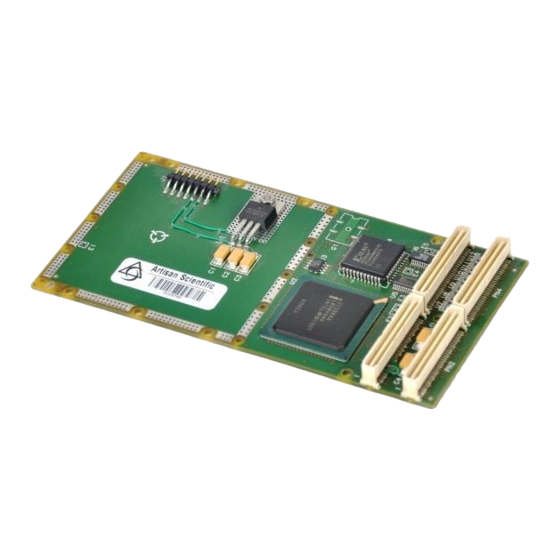
- Page 1 (217) 352-9330 | Click HERE Find the Curtiss-Wright / DY-4 OBYC3-310965-000 at our website:...
- Page 2 Document Number: 809524 Version: Date: February 2009 PCI/PMC UTREACH XPANSION YSTEM ’ ANUAL Curtiss-Wright Controls Embedded Computing 333 Palladium Drive Ottawa, Ontario, Canada K2V 1A6 (613) 599-9199 Artisan Scientific - Quality Instrumentation ... Guaranteed | (888) 88-SOURCE | www.artisan-scientific.com...
- Page 3 Updated to correct SVME/DMV-210 P0 pinout table (see Table 2.6 on page 2-11). Updated to correct SVME/DMV-210 P2 pinout table (see Table 2.8 on page 2-13). February 2009 Updated to address CR#26124. See “Install PMC-605 on Basecard” on page A-3 for corrected cross reference to document number 808335. 809524 V...
- Page 4 The information in this document is subject to change without notice and should not be construed as a commitment by Curtiss-Wright Controls, Inc. While reasonable precautions have been taken, Curtiss-Wright Controls, Inc. assumes no responsibility for any errors that may appear in this document.
- Page 5 PCI/PMC E ’ UTREACH XPANSION YSTEM ANUAL URTISS RIGHT ONTROLS MBEDDED OMPUTING 809524 V 2009 ERSION EBRUARY Artisan Scientific - Quality Instrumentation ... Guaranteed | (888) 88-SOURCE | www.artisan-scientific.com...
-
Page 6: Table Of Contents
RIGHT ONTROLS MBEDDED OMPUTING ABLE OF ONTENTS 1. PMC-605 PCI-P0 Bridge Module ................1-1 General Description ......................1-1 Summary of Features ...................... 1-3 PCI-P0 Bridge Description ......................1-4 21554 PCI-to-PCI-Bridge Controller ................... 1-4 Primary and Secondary PCI Buses ..................1-4 PCI-P0 Bus Arbitration ..................... 1-5 PCI-P0 Bus Clock ...................... - Page 7 SVME/DMV-210 Transparent PCI-PCI Bridging ..............4-1 PMC-605 Terminology ..................... 4-2 Example: Transferring Data Between Two SBCs ............... 4-3 Serial EEPROM Configuration.................... 4-3 SVME/DMV-179 GPM Map Command With PMC-605 Installed ..........4-5 Base Address Register Initialization................... 4-7 Primary BAR Configuration....................4-8 Translated Base Register Configuration................4-9 Address Map for Local PCI and P0 Buses ................4-11...
- Page 8 ONTROLS MBEDDED OMPUTING IST OF IGURES Figure 1.1: Sample Application of PMC-605 PCI-P0 Bridge Module..........1-1 Figure 1.2: PMC-605 Functional Block Diagram ................ 1-2 Figure 1.3: Primary and Secondary PCI Buses ................1-4 Figure 1.4: Bus Arbitration and Signal Direction ............... 1-5 Figure 1.5:...
- Page 9 PCI/PMC E ’ UTREACH XPANSION YSTEM ANUAL URTISS RIGHT ONTROLS MBEDDED OMPUTING 809524 R 2009 VIII EVISION EBRUARY Artisan Scientific - Quality Instrumentation ... Guaranteed | (888) 88-SOURCE | www.artisan-scientific.com...
- Page 10 URTISS RIGHT ONTROLS MBEDDED OMPUTING IST OF ABLES Table 1.1: Clock Source Configurations .................. 1-7 Table 1.2: Local Control and Status Register (LCSR) .............. 1-10 Table 1.3: Environmental Specification Limits and Ruggedization Levels ........1-12 Table 1.4: Pn1/Pn2 Pin Assignments ..................1-14 Table 1.5: Pn3 Pin Assignments ..................
- Page 11 PCI/PMC E ’ UTREACH XPANSION YSTEM ANUAL URTISS RIGHT ONTROLS MBEDDED OMPUTING 809524 R 2009 EVISION EBRUARY Artisan Scientific - Quality Instrumentation ... Guaranteed | (888) 88-SOURCE | www.artisan-scientific.com...
- Page 12 Chapter 2 - SVME/DMV-210 Carrier Card. Describes the features, functions, and pin assignments of the SVME/DMV-210 Carrier Card. Chapter 3 - PCI-P0 Development Backplane. Describes the PMC-605’s PCI-P0 2 and 3 slot development backplanes. Chapter 4 - System Configuration. Explains how to program the base address registers of the PMC-605 and lists the default contents of the EEPROM device.
- Page 13 PCI/PMC E ’ UTREACH XPANSION YSTEM ANUAL URTISS RIGHT ONTROLS MBEDDED OMPUTING ONVENTIONS SED IN THIS ANUAL This document and the accompanying documents in the documentation package use various icon conventions and abbreviations to make the documents clearer and easier to read. These conventions cover typography for such elements as sample software code and keystrokes, signal meanings, and graphical elements for important information such as warnings or cautions.
- Page 14 URTISS RIGHT ONTROLS MBEDDED OMPUTING Table 3 lists the abbreviations used to describe the size of a memory device or a range of Abbreviations addresses. 3: Abbreviations ABLE Abbreviation Convention 1 Kbyte 1,024 bytes 1 Mbyte 1,024 Kbytes 1 Gbyte 1,024 Mbytes Unless otherwise stated, all memory addresses are shown in hexadecimal notation.
- Page 15 • Repair and Warranty • Software Upgrade Program • Lifecycle Support Curtiss-Wright Controls Embedded Computing’s standard warranty provides one-year Repair and coverage of parts and labor and also features: Warranty Information • A repair turnaround target of 15 business days •...
-
Page 16: Figure 1.1: Sample Application Of Pmc-605 Pci-P0 Bridge Module
• Providing a private PCI data path to custom I/O cards. Figure 1.1 shows a sample application of the PMC-605. The two SBCs use the PMC-605 to access each others’ shared PCI resources while the SVME/DMV-210 Carrier Card extends the PCI bus of each single board computer with additional I/O capabilities. - Page 17 PCI/PMC E ’ UTREACH XPANSION YSTEM ANUAL URTISS RIGHT ONTROLS MBEDDED OMPUTING 1.2: PMC-605 Functional Block Diagram IGURE Intel 21554 Embedded PCI Bridge Controller Secondary PCI Bus Primary PCI Bus Secondary Primary Bus PCI Int Arbiter Functions Configuration Settings Serial EEPROM...
-
Page 18: Pmc-605 Pci-P0 Bridge Module
PCI-P0 backplane’s System Slot. The PMC-605 uses a parallel arbitration scheme. The PMC-605 can generate a PCI bus clock for the PCI-P0 bus or receive it from an external PCI Bus Clock source. The PCI bus clock is dynamically enabled when placed in the PCI-P0 backplane’s System Slot and is disabled when placed in a Peripheral Slot. -
Page 19: Pci-P0 Bridge Description
RIMARY AND ECONDARY USES The PMC-605’s Primary PCI bus runs through the P4 connector to the P0 connector on the basecard. The Primary PCI bus runs at 33 MHz and supports 32-bit addressing and data transfers. The Secondary PCI bus is connected to the host basecard’s local PCI bus. The Secondary PCI bus runs at 33 MHz and supports 64-bit addressing and data transfers. -
Page 20: Pci-P0 Bus Arbitration
The PMC-605 uses a parallel arbitration scheme in which each card on the PCI-P0 bus is free Arbitration to request the use of the bus at any time. The PMC-605 acting as bus arbiter grants the bus Scheme on a “first come, first serve” basis. -
Page 21: Pci-P0 Bus Clock
CLKDIS must not be left open circuit because it is an input to the CPLD which does not have a pull-up on it. Inputs should not be left floating. The PMC-605 may not be detected by the host processor if this line is left open. - Page 22 PMC-605 module operate at the same clock speed. Asynchronous System Slot The PMC-605 in the system slot receives a 33 MHz clock source from its host card to provide timing for its secondary side. The PMC-605’s primary bus uses a clock source generated by its on-board oscillator (see Note) and routes this second clock over the PCI-P0 bus.
-
Page 23: Pci-P0 System Slot Termination
PMC-605 with the PCI-P0 Development Backplane. The term System Slot Controller refers to a PMC-605 when it is configured to provide PCI bus arbitration on the PCI-P0, distribute the PCI Bus clock across the backplane, and provide termination of specific signals. -
Page 24: Reset
Reset signal from the host or it can be initiated from the host through software. The PMC-605 does not accept resets from the PCI-P0 bus, regardless of the state of TERMDIS. If an external PMC-605 reset is required, this must be done via the host basecard’s VME interface. -
Page 25: Serial Eeprom
21554 after power-up or card reset. Refer to Chapter 4 of this manual and Appendix A of the V8 Foundation Firmware User’s Manual (808006) for more information. The PMC-605 has a green power-on LED that is software-controllable via the Local Control and Status Register (LCSR). After Power up or reset, the LED will be initially illuminated. The LED is extinguished when the PMC605 is successfully initialized and its diagnostics passed by FF/W. -
Page 26: Dimensions
Component Side Solder Side 21554 CPLD IMENSIONS The PMC-605 is built on a standard PCI Mezzanine Card (PMC) Printed Wiring Board (PWB) and is VITA 20 compliant. ATING ONNECTORS The connectors Pn1, Pn2, Pn3, and Pn4 are compliant with IEEE P1386. -
Page 27: Electrical Characteristics
LECTRICAL HARACTERISTICS The PMC-605 is powered from the basecard’s +5 V rail and operates with a steady state input voltage of 5.0 +/- 0.25 volts DC with a maximum current of 0.75 A. It draws less than 4 watts of power. An on-board regulator provides +3.3 V for the 21554 PCI to PCI Bridge device. -
Page 28: Connector Pin Assignments
PMC-605 PCI-P0 B URTISS RIGHT ONTROLS MBEDDED OMPUTING RIDGE ODULE ONNECTOR SSIGNMENTS ONNECTOR OCATIONS The locations of the Pn1, Pn2, Pn3, Pn3 and J1 connectors are shown in Figure 1.8. 1.8: Connector Locations IGURE 809524 R 2009 1-13 EVISION EBRUARY... -
Page 29: Pn1/Pn2 Pin Assignments
PCI/PMC E ’ UTREACH XPANSION YSTEM ANUAL URTISS RIGHT ONTROLS MBEDDED OMPUTING SSIGNMENTS 1.4: Pn1/Pn2 Pin Assignments ABLE Pn1 32-bit PCI Pn2 32-bit PCI Pin # Signal Name Signal Name Pin # Pin # Signal Name Signal Name Pin # -12V +12V TRST#... -
Page 30: Pn3 Pin Assignments
PMC-605 PCI-P0 B URTISS RIGHT ONTROLS MBEDDED OMPUTING RIDGE ODULE SSIGNMENTS 1.5: Pn3 Pin Assignments ABLE Pin # Signal Name Signal Name Pin # PCI-RSVD CBE7# CBE6# CBE5# CBE4# V(I/O) PAR64 AD[63] AD[62] AD[61] AD[60] AD[59] AD[58] AD[57] V(I/O) AD[56]... -
Page 31: Pn4 Pin Assignments
PCI/PMC E ’ UTREACH XPANSION YSTEM ANUAL URTISS RIGHT ONTROLS MBEDDED OMPUTING SSIGNMENTS 1.6: Pn4 Pin Assignments ABLE Pin # Signal Name Signal Name Pin # RST# PCLK0 REQ0# GNT0# INTA# PCLK1 REQ1# DEVSEL# GNT1# SERARB IRDY# TRDY# +5 V SERR# IDSEL PERR#... -
Page 32: J1 Test Jtag Port
IGURE SVME/DMV-179 PMC-605 Table 1.8 describes the P0 connector of an SVME/DMV-179 with a PMC-605 mounted in the PMC1 interface. The shaded boxes represent PCI signals provided by the PMC-605 when plugged into the System Slot on the PCI-P0 backplane. - Page 33 AD26 AD28 AD29 AD30 AD31 PIO(11) To support PMC-605 I/O via the SVME/DMV-179 P0 connector, the SVME/DMV-179 must be ordered from the factory with support for either I/O Mode 1 or I/O Mode 4. Note 1-18 809524 R 2009 EVISION EBRUARY Artisan Scientific - Quality Instrumentation ...
-
Page 34: General Description
VMEBus alone cannot meet the current demand. The SVME/DMV-210 is used in conjunction with the PMC-605 to expand the PCI bus of a processor card (a Single Board Computer or SBC) through the P0 connector. Two SVME/DMV-210 cards can be supported by a single SBC, expanding the available PMC support to a total of five modules. -
Page 35: Summary Of Features
PCI/PMC E ’ UTREACH XPANSION YSTEM ANUAL URTISS RIGHT ONTROLS MBEDDED OMPUTING UMMARY OF EATURES The SVME/DMV-210 has the following major features: Initiator-Target PCI Bridge Interface (Intel 21154 PCI-PCI bridge). Bridge Device • P0 PCI data bus: 32-bit 25 MHz minimum (33 MHz typical) •... -
Page 36: Pci-P0 Bridge Description
SVME/DMV-210 C URTISS RIGHT ONTROLS MBEDDED OMPUTING ARRIER PCI-P0 B RIDGE ESCRIPTION The SVME/DMV-210 uses the Intel 21154 PCI to PCI transparent bridge to connect the PMC modules to the PCI-P0 bus. The bridge has a 32-bit, 25 MHz (minimum, 33 MHz typical) Initiator-Target PCI primary interface and a 64-bit, 25 MHz (minimum, 33 MHz typical) Initiator-Target PCI secondary interface. -
Page 37: Pci Jtag Test Signals
PCI/PMC E ’ UTREACH XPANSION YSTEM ANUAL URTISS RIGHT ONTROLS MBEDDED OMPUTING PCI JTAG T IGNALS The SVME/DMV-210 does not support PCI JTAG test signals. PMC B IGNALS The PMC Busmode[4:2] signals are tied to the appropriate logic level on the SVME/DMV-210: •... -
Page 38: Physical, Electrical, And Environmental Characteristics
SVME/DMV-210 C URTISS RIGHT ONTROLS MBEDDED OMPUTING ARRIER HYSICAL LECTRICAL AND ENVIRONMENTAL HARACTERISTICS Figure 2.3 shows the location of the major components and the mating connectors on the SVME/DMV-210. 2.3: SVME/DMV-210 Physical Layout IGURE PMC Site 1 PMC Site 2 IMENSIONS The SVME/DMV-210 is built on a standard VMEbus 6U Printed Wiring Board (PWB) and is VITA 20 compliant. -
Page 39: Electrical Characteristics
PCI/PMC E ’ UTREACH XPANSION YSTEM ANUAL URTISS RIGHT ONTROLS MBEDDED OMPUTING LECTRICAL HARACTERISTICS The maximum current of the SVME/DMV-210 at +5 V is 1000 mA (PMC cards not included). NVIRONMENTAL HARACTERISTICS Table 2.1 shows the complete range of environmental specification limits used to categorize the ruggedization levels of CWCEC products. -
Page 40: Connector Pin Assignments
SVME/DMV-210 C URTISS RIGHT ONTROLS MBEDDED OMPUTING ARRIER ONNECTOR SSIGNMENTS PMC S 1: J ONNECTORS 2.2: PMC Site 1: Pin Assignments (Jn1 and Jn2) ABLE PMC Site 1: Jn1 32 Bit PCI PMC Site 1: Jn2 32 Bit PCI Pin # Signal Name Signal Name Pin #... -
Page 41: Pmc Site 1: Jn3 And Jn4 Connectors
PCI/PMC E ’ UTREACH XPANSION YSTEM ANUAL URTISS RIGHT ONTROLS MBEDDED OMPUTING PMC S 1: J ONNECTORS 2.3: PMC Site 1: Pin Assignments (Jn3 and Jn4) ABLE PMC Site 1: Jn3 32 Bit PCI PMC Site 1: Jn4 32 Bit PCI Pin # Signal Name Signal Name... -
Page 42: Pmc Site 2: Jn1 And Jn2 Connectors
SVME/DMV-210 C URTISS RIGHT ONTROLS MBEDDED OMPUTING ARRIER PMC S 2: J ONNECTORS 2.4: PMC Site 2: Pin Assignments (Jn1 and Jn2) ABLE PMC Site 2: Jn1 32 Bit PCI PMC Site 2: Jn2 32 Bit PCI Pin # Signal Name Signal Name Pin # Pin #... -
Page 43: Pmc Site 2: Jn3 And Jn4 Connectors
PCI/PMC E ’ UTREACH XPANSION YSTEM ANUAL URTISS RIGHT ONTROLS MBEDDED OMPUTING PMC S 2: J ONNECTORS 2.5: PMC Site 2: Pin Assignments (Jn3 and Jn4) ABLE PMC Site 1: Jn3 32 Bit PCI PMC Site 1: Jn4 32 Bit PCI Pin # Signal Name Signal Name... -
Page 44: Vme P0 Connector Pin Assignments
SVME/DMV-210 C URTISS RIGHT ONTROLS MBEDDED OMPUTING ARRIER VME P0 C ONNECTOR SSIGNMENTS The pin assignments for the VME P0 connector are shown in Table 2.6. 2.6: VME P0 Connector Pin Assignments ABLE Pin # PMC1_IO[11] PMC1_IO[10] PMC1_IO[9] PMC1_IO[8] PMC1_IO[7] PMC1_IO[16] PMC1_IO[15] PMC1_IO[14]... -
Page 45: Vme P1 Connector Pin Assignments
PCI/PMC E ’ UTREACH XPANSION YSTEM ANUAL URTISS RIGHT ONTROLS MBEDDED OMPUTING VME P1 C ONNECTOR SSIGNMENTS The pin assignments for the VME P1 connector are shown in Table 2.7. 2.7: Pin Assignments for VME P1 Connector ABLE Pin # P1A_NC1 P1B_NC1 P1C_NC1... -
Page 46: Vme P2 Connector Pin Assignments
SVME/DMV-210 C URTISS RIGHT ONTROLS MBEDDED OMPUTING ARRIER VME P2 C ONNECTOR SSIGNMENTS The pin assignments for the VME P2 connector are shown in Table 2.8. 2.8: Pin Assignments for VME P2 Connector ABLE Pin # PMC2_IO[02] PMC2_IO[01] PMC1_IO[19] PMC1_IO[20] PMC2_IO[04] PMC2_IO[03] PMC1_IO[21]... - Page 47 PCI/PMC E ’ UTREACH XPANSION YSTEM ANUAL URTISS RIGHT ONTROLS MBEDDED OMPUTING Table 2.8 shows generic PMC module signal names (e.g. PMC2_IO[02]) for the PMC modules that may (or may not) be installed in either PMC Site 1 or PMC Site 2 on the SVME/DMV-210 Carrier Card.
-
Page 48: Pci-P0 Development Backplane
PCI-P0 D EVELOPMENT ACKPLANE ENERAL ESCRIPTION The PCI-P0 development backplane comes in 2 and 3 slot versions (order numbers BPL-605- 002 and BPL-605-003). The slots are labelled from left to right: System Slot 0, Peripheral Slot 1, and Peripheral Slot 2. 3.1: PCI-P0 Development Backplane Slot Locations (3 Slot Version) IGURE Pin A1... -
Page 49: Backplane Jumper Configurations
Ground). The other PMC-605s should have bus arbitration disabled (ARBIS signal connected to Vcc). While each PMC-605 is capable of acting as the bus arbiter, the BPL-605-002 and BPL-605- 003 backplanes are tracked so that only the System Slot supports a bus arbiter. -
Page 50: Figure 3.2: Bus Arbiter Jumper Locations
PCI-P0 D URTISS RIGHT ONTROLS MBEDDED OMPUTING EVELOPMENT ACKPLANE 3.1: Bus Arbiter Jumper Settings ABLE 2 Slot Backplane 3 Slot Backplane Recommended Setting: Recommended Setting: Set 605 in System Slot 0 as Arbiter: Set 605 in System Slot 0 as Arbiter: Slot 0. -
Page 51: Pci Bus Clock Jumper Settings
LOCK UMPER ETTINGS Each PCI-P0 system requires one and only one PMC-605 configured to provide a clock source (CLKDIS signal connected to Ground). The other PMC-605s should have clock output disabled (CLKDIS signal connected to Vcc). While each PMC-605 card is capable of providing a clock source, the BPL-605-002 and BPL- 605-003 backplanes are tracked so that only the System Slot can provide a clock source. -
Page 52: System Slot Termination Jumper Settings
ERMINATION UMPER ETTINGS Each PCI-P0 system requires one and only one PMC-605 configured to terminate PCI bus signals (TERMDIS signal connected to Ground). The other PMC-605s should not be set to terminate bus signals (TERMDIS signal connected to Vcc). While each PMC-605 is capable of terminating bus signals, the BPL-605-002 and BPL-605- 003 backplanes are tracked so that only the System Slot supports signal termination. -
Page 53: Figure 3.4: Bus Termination Jumper Locations
PCI/PMC E ’ UTREACH XPANSION YSTEM ANUAL URTISS RIGHT ONTROLS MBEDDED OMPUTING 3.4: Bus Termination Jumper Locations IGURE Slot 1 Slot 0 Slot 2 Slot 1 Slot 0 J1-A1 J1-A1 Rear View - 2 Slot Backplane Rear View - 3 Slot Backplane (BPL-605-002) (BPL-605-003) The 95-pin connectors mounted on the opposite side of the above circuit cards plug into the... -
Page 54: Pci-P0 Backplane Pin Assignments
PCI-P0 D URTISS RIGHT ONTROLS MBEDDED OMPUTING EVELOPMENT ACKPLANE PCI-P0 B ACKPLANE SSIGNMENTS ACKPLANE ONFIGURATION In a 2 slot backplane, each slot has 4 configuration pins that are independent of other slots. These control: arbiter functions, clock source, line termination and bus arbitration. 3.4: 2 Slot Backplane Configuration Pins ABLE... -
Page 55: Slot Backplane System Slot 0 Pin Assignments
AD27 AD26 AD28 AD29 AD30 AD31 basecard signal Pins carrying PMC-605 signals are cut short to prevent the PCI-P0 bus from being over- extended when a cable is attached to the development backplane. Note 809524 R 2009 EVISION EBRUARY Artisan Scientific - Quality Instrumentation ... Guaranteed | (888) 88-SOURCE | www.artisan-scientific.com... -
Page 56: Slot Backplane Peripheral Slot 1 Pin Assignments
AD27 AD26 AD28 AD29 AD30 AD31 basecard signal Pins carrying PMC-605 signals are cut short to prevent the PCI-P0 bus from being over- extended when a cable is attached to the development backplane. Note 809524 R 2009 EVISION EBRUARY Artisan Scientific - Quality Instrumentation ... Guaranteed | (888) 88-SOURCE | www.artisan-scientific.com... -
Page 57: Slot Backplane Configuration Pins
PCI/PMC E ’ UTREACH XPANSION YSTEM ANUAL URTISS RIGHT ONTROLS MBEDDED OMPUTING ACKPLANE ONFIGURATION In a 3 slot backplane, each slot has 4 configuration pins that are independent of other slots. These control: arbiter functions, clock source, line termination and bus arbitration. 3.7: 3 Slot Backplane Configuration Pins ABLE... - Page 58 AD27 AD26 AD28 AD29 AD30 AD31 basecard signal Pins carrying PMC-605 signals are cut short to prevent the PCI-P0 bus from being over- extended when a cable is attached to the development backplane. Note 809524 R 2009 3-11 EVISION EBRUARY...
- Page 59 AD27 AD26 AD28 AD29 AD30 AD31 basecard signal Pins carrying PMC-605 signals are cut short to prevent the PCI-P0 bus from being over- extended when a cable is attached to the development backplane. Note 3-12 809524 R 2009 EVISION EBRUARY...
- Page 60 AD27 AD26 AD28 AD29 AD30 AD31 basecard signal Pins carrying PMC-605 signals are cut short to prevent the PCI-P0 bus from being over- extended when a cable is attached to the development backplane. Note 809524 R 2009 3-13 EVISION EBRUARY...
- Page 61 PCI/PMC E ’ UTREACH XPANSION YSTEM ANUAL URTISS RIGHT ONTROLS MBEDDED OMPUTING 3-14 809524 R 2009 EVISION EBRUARY Artisan Scientific - Quality Instrumentation ... Guaranteed | (888) 88-SOURCE | www.artisan-scientific.com...
-
Page 62: System Integration
21554 Embedded PCI-to-PCI Bridge, number 278210-001, downloadable from the Intel website at Cross Reference http://developer.intel.com. For a complete list and description of the Foundation Firmware used with the PMC-605, refer to Appendix A of the Foundation Firmware User’s Manual, document number 808006. PMC-605 N PCI-PCI B... -
Page 63: Pmc-605 Terminology
ONTROLS MBEDDED OMPUTING PMC-605 T ERMINOLOGY The PCI local bus refers to the host SBC’s PCI local bus and is connected to the secondary side of the 21554 PCI bridge. The PCI-P0 bus connects to the P0 backplane and to the primary side of the 21554. -
Page 64: Serial Eeprom Configuration
ERIAL ONFIGURATION The PMC-605 is provided with a serial EEPROM to enable configuration of certain registers at power up or reset. This serial EEPROM is programmed at the factory with default values to provide a basic configuration for the 21554 configuration registers. These default values can be changed using the PMC-605 service Pmc605_writeSeeprom. - Page 65 PCI/PMC E ’ UTREACH XPANSION YSTEM ANUAL URTISS RIGHT ONTROLS MBEDDED OMPUTING 4.1: Serial EEPROM Factory Default Values ABLE Offset Data Description 0x80 Preload enable bit 7- Warning: Do not change this value 0x00 0x00 0x00 0x00 Primary Class code 0x80 0x06 0xD4...
-
Page 66: Svme/Dmv-179 Gpm Map Command With Pmc-605 Installed
0x00 0x00 0x00 These default values listed above can be changed using the PMC-605 service Pmc605_writeSeeprom. Refer to Appendix A of the Foundation Firmware User’s Manual (document number 808006) for a complete description of the PMC-605 FF/W Services. Cross Reference... - Page 67 PCI/PMC E ’ UTREACH XPANSION YSTEM ANUAL URTISS RIGHT ONTROLS MBEDDED OMPUTING 40000000* map Hardware map for the SVME/DMV-179 Base Addr. Size LM Addr. ---------- ---------- ---------- A24: 0x00400000 0x00080000 0x00000000 A32: 0x40000000 0x07FFF000 0x00000000 ---------- ---------- ---------- CFI1-4Mx16: 0xFF000000 0x01000000 CFI1-4Mx16: 0xFE000000 0x01000000 DRAM: 0x00000000 0x08000000 NOVRAM: 0xF4008000 0x00008000...
-
Page 68: Base Address Register Initialization
/*Upstream I/O BAR*/ Alternatively, the Secondary PCI Configuration register defaults can be examined using the GPM command 'PCID'. For example, to display the contents of the PMC-605 Configuration registers in the PMC slot 1 on a SVME/DMV-179: At the GPM prompt, type:... -
Page 69: Primary Bar Configuration
RIMARY ONFIGURATION Once the Secondary BARs are configured, then the Primary BARs of the PMC-605 must be configured. This can be achieved by any device with access to the PCI-P0 bus configuration space. In this example the host SBC in slot 1 will configure the primary BARs of its own PMC- 605 via the PMC-605’s Secondary interface configuration space and the Primary BARs of the... -
Page 70: Translated Base Register Configuration
/*Enable the Master PMC605 to respond to PCI cycles and ability to act as master on the PCI-P0 bus*/ PciConfigWrite(busNo, deviceNo,functionNo,0x44,0x0007,sizeof(uint16)); Now the Primary BARS on the slave PMC-605 have to be set using the Configure Slave’s PMC-605 service Pmc605_pciP0ConfigWrite(). The parameters to access a PMC-605’s... - Page 71 PCI/PMC E ’ UTREACH XPANSION YSTEM ANUAL URTISS RIGHT ONTROLS MBEDDED OMPUTING Your SBC’s Programmer’s Reference Manual provides details of the System Memory Map showing the address of the RAM as seen by a local PCI bus Master. Cross Reference The parameters to set up the translated base registers are as follows: /*Set the Downstream I/O or Mem.
-
Page 72: Address Map For Local Pci And P0 Buses
URTISS RIGHT ONTROLS MBEDDED OMPUTING YSTEM NTEGRATION P0 B DDRESS AP FOR OCAL USES With all the necessary registers now configured the address map for the local PCI and P0 buses appears as shown in Figure 4.5. 4.5: Master-Slave Memory Mappings IGURE PCI-P0 I/O map Master SBC Address map... -
Page 73: Pci-P0 Configuration Space Addressing
DDRESSING XAMPLE Suppose you wish to read the Primary CSR and Downstream Memory 0 Base Address Register (BAR) on the PMC-605 in slot 2. Using the PMC-605 service Pmc605_pciPoConfigRead, you would construct the address as follows: #include pmc605.h #include dy4std.h uint32 busNo = 0;... - Page 74 In order to generate a Type 1 configuration cycle to access configuration space on a PCI bus on the downstream side of a PCI to PCI bridge other than a PMC-605, the bus number must be greater than zero. In this instance the values are passed straight through to the PCI-P0 bus as follows: 4.7: Type 1 Configuration Cycle Example...
- Page 75 PCI/PMC E ’ UTREACH XPANSION YSTEM ANUAL URTISS RIGHT ONTROLS MBEDDED OMPUTING 4-14 809524 R 2009 EVISION EBRUARY Artisan Scientific - Quality Instrumentation ... Guaranteed | (888) 88-SOURCE | www.artisan-scientific.com...
-
Page 76: Installation Instructions
This appendix explains how to install and configure the Outreach Expansion System. The Outreach Expansion System consists of: • one or more Single Board Computers, each equipped with a PMC-605 module • one or more SVME/DMV-210 Carrier Cards, each equipped with one or two PMC mod- ules •... -
Page 77: Unpack Cards
Refer to your SBC’s Getting Started Manual for information selecting jumper settings and configuring your SBCs. The PMC-605 and the SVME/DMV-210 have no user-definable jumper settings. Configuration is done via the PCI-P0 development backplane. The PCI-P0 development backplane (identified as either BPL-605-002 or BPL-605-003) has jumper settings that configure the bus arbiter, the arbitration scheme, the system clock, and the system controller functions. -
Page 78: Install Pmc-605 On Basecard
NSTALL ASECARD The PMC-605 should only be installed on an SBC in the PMC slot that routes the PMC-605’s P4 connector to the SBC’s P0 connector. The PMC-605 will not operate correctly if installed in a different basecard PMC slot position. -
Page 79: Attach The Pci-P0 Development Backplane
MBEDDED OMPUTING Insert the first SBC with PMC-605 card in Slot 1, the left-most slot in the VME chassis, if you Choosing Slot want it to be the VMEbus System Controller (SYSCON). If you intend to use another card as Locations the SYSCON, place the SBC with PMC-605 in the left-most unoccupied slot. -
Page 80: Connect Basecard To Terminal
Power on the VME chassis. The SBC will power on and run its internal diagnostics (which includes diagnostics for the PMC-605). The LED on the PMC-605 will initially be illuminated. When the PMC-605 is successfully initialized and its diagnostics passed by FF/W, the LED is extinguished. -
Page 81: Install Bsp
PCI/PMC E ’ UTREACH XPANSION YSTEM ANUAL URTISS RIGHT ONTROLS MBEDDED OMPUTING NSTALL Once the hardware is correctly configured and installed in the chassis, the next step is to install the host card’s board support package software. See the BSP Software User’s Manual for more information. -
Page 82: Index
4-3 block diagram features PMC-605 1-2 PMC-605 1-3 SVME/DMV-210 2-2 SVME/DMV-210 2-2 block diagram, PMC-605 1-2 boundary scan (JTAG) 1-3 bus arbiter 1-5 Bus Arbiter jumper settings 3-3 initial screen message A-5 bus arbitration 1-3 input voltage 1-12... - Page 83 ANUAL URTISS RIGHT ONTROLS MBEDDED OMPUTING jumper configurations 3-2 PMC-605 1-12 preload enable bit 4-3 Primary PCI bus 1-4 LED 1-3, 1-10 LED behaviour during power-up A-5 Local Control and Status Register (LCSR) 1-10 random vibration 1-12, 2-6 Local PCI Address Map 4-7...
- Page 84 URTISS RIGHT ONTROLS MBEDDED OMPUTING VME P0 Connector pin assignments 2-11 VME P1 Connector pin assignments 2-12 VME P2 Connector pin assignments 2-13 809524 V 2009 ERSION EBRUARY Artisan Scientific - Quality Instrumentation ... Guaranteed | (888) 88-SOURCE | www.artisan-scientific.com...
- Page 85 PCI/PMC E ’ UTREACH XPANSION YSTEM ANUAL URTISS RIGHT ONTROLS MBEDDED OMPUTING 809524 V 2009 ERSION EBRUARY Artisan Scientific - Quality Instrumentation ... Guaranteed | (888) 88-SOURCE | www.artisan-scientific.com...
Need help?
Do you have a question about the PMC-605 and is the answer not in the manual?
Questions and answers