Table of Contents
Advertisement
Advertisement
Table of Contents

Subscribe to Our Youtube Channel
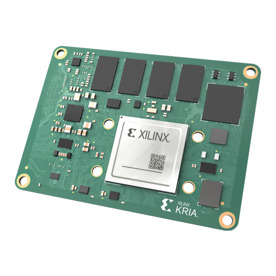
Summary of Contents for Xilinx Kria K26 SOM
- Page 1 Kria SOM Carrier Card Design Guide UG1091 (v1.0) April 20, 2021...
-
Page 2: Revision History
Revision History Revision History The following table shows the revision history for this document. Section Revision Summary 4/20/2021 Version 1.0 Initial release. UG1091 (v1.0) April 20, 2021 www.xilinx.com Send Feedback Carrier Card Design for Kria SOM... -
Page 3: Table Of Contents
Chapter 4: Hardware Configuration Using Vivado Tools ......55 Vivado Tools Board File......................55 Vivado Software SOM Connector Abstraction............... 56 SOM Vivado Tools XDC Files.....................56 Appendix A: Additional Resources and Legal Notices ......57 UG1091 (v1.0) April 20, 2021 www.xilinx.com Send Feedback Carrier Card Design for Kria SOM... - Page 4 Xilinx Resources.........................57 Documentation Navigator and Design Hubs.................57 References..........................57 Please Read: Important Legal Notices................... 58 UG1091 (v1.0) April 20, 2021 www.xilinx.com Send Feedback Carrier Card Design for Kria SOM...
-
Page 5: Chapter 1: Introduction
Xilinx product documentation to help the reader find more detailed technical information available in corresponding technical reference manuals, software design guides, and thermal design guides. The Kria K26 SOM is used an example throughout the guide and is shown in the following block diagram. - Page 6 Chapter 1: Introduction Figure 1: K26 SOM Block Diagram Connector 1 Connnector 2 x21 HDIO x32 HPIO (x16 differential pairs) Xilinx MPSoC Programmable PCIe v3.1 100Gb Logic OCM Memory 2-way Cache Non-Coherent PL SysMon Coherent Master Master I/O Coherent Block RAM...
-
Page 7: Chapter 2: Electrical Design Considerations
• High-density I/O (HDIO) bank signals • GTH high-speed serial transceiver signals • Power system Signal Naming Conventions The SOM240 connectors adopt the naming conventions outlined in the following table. UG1091 (v1.0) April 20, 2021 www.xilinx.com Send Feedback Carrier Card Design for Kria SOM... -
Page 8: Som240_1 Connector Pinout
The SOM240_1 connector provides access to two MIO banks (MIO501, MIO502), HPIO bank 66 (HPA), HDIO bank 45 (HDA), and the PS-GTR transceivers (MIO505). It also provides sideband signals for configuration and operation of the board. UG1091 (v1.0) April 20, 2021 www.xilinx.com Send Feedback Carrier Card Design for Kria SOM... - Page 9 MIO36 MIO27 MODE3_C2M MIO37 MIO29 MIO28 Reserved MIO30 Reserved MIO38 MIO31_SHUTDOWN MIO44 MIO39 MIO45 MIO41 MIO40 MIO47 MIO46 MIO42 MIO48 MIO43 MIO50 MIO49 MIO52 MIO51 MIO53 UG1091 (v1.0) April 20, 2021 www.xilinx.com Send Feedback Carrier Card Design for Kria SOM...
- Page 10 HPIO on bank 66 HPA06_N HPIO on bank 66 Ground HPA_CLK0_P HPIO global clock pin on bank 66 HPA_CLK0_N HPIO global clock pin on bank 66 UG1091 (v1.0) April 20, 2021 www.xilinx.com Send Feedback Carrier Card Design for Kria SOM...
- Page 11 PS MIO signal on bank 502 Ground MIO73 PS MIO signal on bank 502 MIO74 PS MIO signal on bank 502 MIO75 PS MIO signal on bank 502 Ground Ground UG1091 (v1.0) April 20, 2021 www.xilinx.com Send Feedback Carrier Card Design for Kria SOM...
- Page 12 HDIO on bank 45 Ground HDA15 HDIO on bank 45 HDA16_CC HDIO clock-capable pin on bank 45 HDA17 HDIO on bank 45 Ground PS_ERROR_OUT_M2C PS error indication from SOM UG1091 (v1.0) April 20, 2021 www.xilinx.com Send Feedback Carrier Card Design for Kria SOM...
- Page 13 PS-GTR lane 2 RX Ground Ground GTR_DP0_M2C_P PS-GTR lane 0 TX GTR_DP0_M2C_N PS-GTR lane 0 TX Ground VCC_SOM SOM main supply voltage, +5V Connector Row C Ground Ground UG1091 (v1.0) April 20, 2021 www.xilinx.com Send Feedback Carrier Card Design for Kria SOM...
- Page 14 PS MIO signal on bank 501 MIO49 PS MIO signal on bank 501 Ground MIO55 PS MIO signal on bank 502 MIO56 PS MIO signal on bank 502 UG1091 (v1.0) April 20, 2021 www.xilinx.com Send Feedback Carrier Card Design for Kria SOM...
- Page 15 HPIO on bank 66 Ground HPA14_P HPIO on bank 66 HPA14_N HPIO on bank 66 Ground HDA00_CC HDIO clock-capable pin on bank 45 HDA01 HDIO on bank 45 UG1091 (v1.0) April 20, 2021 www.xilinx.com Send Feedback Carrier Card Design for Kria SOM...
- Page 16 No connect on the SOM Ground Ground GTR_DP3_C2M_P PS-GTR lane 3 RX GTR_DP3_C2M_N PS-GTR lane 3 RX Ground Ground GTR_REFCLK2_C2M_P PS-GTR REFCLK2 input GTR_REFCLK2_C2M_N PS-GTR REFCLK2 input Ground Ground UG1091 (v1.0) April 20, 2021 www.xilinx.com Send Feedback Carrier Card Design for Kria SOM...
-
Page 17: Som240_2 Connector Pinout
HPB08_P HPB14_P HPB08_N HPB07_P HPB14_N HPB00_CC_P HPB07_N HPB00_CC_N HPB12_P HPB02_P HPB12_N HPB05_CC_P HPB02_N HPB_CLK0_P HPB05_CC_N HPB_CLK0_N HPB06_P HPB13_P HPB06_N HPB11_P HPB13_N HPB04_P HPB11_N HPB04_N HPB16_P HPB_18_P UG1091 (v1.0) April 20, 2021 www.xilinx.com Send Feedback Carrier Card Design for Kria SOM... - Page 18 HDC13 HDC01 HDC18 HDC14 HDC06 HDC02 HDC19 HDC07 HDC20 HDC15 HDC08_CC HDC03 HDC16_CC HDC04 HDC21 HDC17 HDC09 HDC05 HDC22 VCCO_HDB HDC10 VCCO_HDC HDC23 VCCO_HDB HDC11 VCCO_HDC UG1091 (v1.0) April 20, 2021 www.xilinx.com Send Feedback Carrier Card Design for Kria SOM...
- Page 19 HPIO on bank 64 Ground HPC19_P HPIO on bank 64 HPC19_N HPIO on bank 64 Ground HPC14_P HPIO on bank 64 HPC14_N HPIO on bank 64 UG1091 (v1.0) April 20, 2021 www.xilinx.com Send Feedback Carrier Card Design for Kria SOM...
- Page 20 GTH Lane 2 TX Ground Ground GTH_DP0_C2M_P GTH Lane 0 RX GTH_DP0_C2M_N GTH Lane 0 RX Ground HPB10_CC_P HPIO on bank 65 HPB10_CC_N HPIO on bank 65 Ground UG1091 (v1.0) April 20, 2021 www.xilinx.com Send Feedback Carrier Card Design for Kria SOM...
- Page 21 HDIO on bank 43 HDB16_CC HDIO clock-capable pin on bank 43 HDB17 HDIO on bank 43 Ground HDC12 HDIO on bank 44 HDC13 HDIO on bank 44 UG1091 (v1.0) April 20, 2021 www.xilinx.com Send Feedback Carrier Card Design for Kria SOM...
- Page 22 HPC17_P HPIO on bank 64 HPC17_N HPIO on bank 64 Ground HPC10_CC_P HPIO clock-capable pin on bank 64 HPC10_CC_N HPIO clock-capable pin on bank 64 Ground UG1091 (v1.0) April 20, 2021 www.xilinx.com Send Feedback Carrier Card Design for Kria SOM...
- Page 23 GTH Lane 1 RX GTH_DP1_C2M_N GTH Lane 1 RX Ground Ground GTH_DP3_M2C_P GTH Lane 3 TX GTH_DP3_M2C_N GTH Lane 3 TX Ground Ground GTH_DP0_M2C_P GTH Lane 0 TX UG1091 (v1.0) April 20, 2021 www.xilinx.com Send Feedback Carrier Card Design for Kria SOM...
- Page 24 HPC I/O voltage rail, 1.0V to 1.8V Ground HDB00_CC HDIO clock-capable pin on bank 43 HDB01 HDIO on bank 43 HDB02 HDIO on bank 43 Ground HDB03 HDIO on bank 43 UG1091 (v1.0) April 20, 2021 www.xilinx.com Send Feedback Carrier Card Design for Kria SOM...
-
Page 25: Supported I/O Standards
• Implement length matching as required by the interface used on individual MIO signal groups defined by the application MIO configuration. • All MIO signals must be 1.8V compatible. UG1091 (v1.0) April 20, 2021 www.xilinx.com Send Feedback Carrier Card Design for Kria SOM... - Page 26 • PS-GTR differential signals to all other signal spacing should be four times the distance between the signal to the nearest GND plane. UG1091 (v1.0) April 20, 2021 www.xilinx.com Send Feedback Carrier Card Design for Kria SOM...
- Page 27 TIP: The K26 SOM device and package delay file is available in the Vivado ® tools. The following table defines the physical length associated with each I/O bank from the Zynq UltraScale+ MPSoC to the corresponding board-to-board connector. UG1091 (v1.0) April 20, 2021 www.xilinx.com Send Feedback Carrier Card Design for Kria SOM...
-
Page 28: Som Configuration And Control Signals
UltraScale+ MPSoC SOM. Power-on Reset (PS_POR_B) Signal This is the Zynq UltraScale+ MPSoC power-on reset signal. In Xilinx documentation this signal is also described as PS_POR_B. The POR_B signal is an active-Low signal that must be asserted during the SOM power-up sequence. - Page 29 The BOOT_MODE pins define the physical device that the Zynq UltraScale+ MPSoCwill read boot firmware from. The boot firmware is prepackaged as a boot.bin, which is a consolidated boot firmware binary constructed using the Xilinx Bootgen tool outlined in the Bootgen User Guide (UG1283).
- Page 30 SOM PS low-power domain (LPD) rails. PWRGD_LPD_M2C is pulled High to 1.80V on the SOM. A carrier card can use this signal to monitor LPD status. UG1091 (v1.0) April 20, 2021 www.xilinx.com Send Feedback Carrier Card Design for Kria SOM...
- Page 31 A carrier card can use this signal as an indication to turn power on for all PL peripherals. UG1091 (v1.0) April 20, 2021 www.xilinx.com Send Feedback Carrier Card Design for Kria SOM...
-
Page 32: Som Mio Design Considerations
If the carrier card design extends this bus, they need to ensure they do not introduce an address conflict with the I2C devices on the SOM. The I2C devices are defined in the corresponding table of the Kria K26 SOM Data Sheet (DS987). - Page 33 RECOMMENDED: The carrier card design should include a UART for board bring-up and initial debug. The Xilinx K26 boot firmware and PetaLinux BSP default the UART interface to MIO36 and MIO37. It is recommended that carrier card designs use this same mapping to be able to use the Xilinx provided software references.
-
Page 34: Som Power
1.764V–1.854V. • If an HDIO bank is configured for the LVDS_25 standard, the V at the SOM connector pin must be within 2.450V–2.575V. UG1091 (v1.0) April 20, 2021 www.xilinx.com Send Feedback Carrier Card Design for Kria SOM... - Page 35 RECOMMENDED: Your carrier card should employ a current sensing device to monitor the input current on the V supply rail that is powering the SOM. Xilinx carrier cards add this current sensing device to CC_SOM the PS I2C bus to minimize I/O.
- Page 36 (1.8V) CCAUX CC_PL_1V80 (0.85V) CCBRAM CC_PL_0V85 The Zynq UltraScale+ MPSoC SYSMON is supported for Linux applications by the Xilinx analog mixed signal (AMS) driver, available in the Xilinx GitHub. The SYSMON is supported for bare-metal applications by the SYSMONPSU driver.
-
Page 37: Chapter 3: Mechanical Design Considerations
SOM. Table 13: K26 SOM Mechanical Specifications Parameter Specification SOM length 77 mm SOM width 60 mm SOM height 10.9 mm Mass 58 grams UG1091 (v1.0) April 20, 2021 www.xilinx.com Send Feedback Carrier Card Design for Kria SOM... - Page 38 Chapter 3: Mechanical Design Considerations Figure 2: K26 SOM Dimensions UG1091 (v1.0) April 20, 2021 www.xilinx.com Send Feedback Carrier Card Design for Kria SOM...
-
Page 39: Pcb Fabrication And Assembly House Requirements
The following image shows that even though placement of the connector shifted by 15% of the pad width, the connector solder ball was still able to self-align to the center of pad. UG1091 (v1.0) April 20, 2021 www.xilinx.com Send Feedback Carrier Card Design for Kria SOM... -
Page 40: Som To Carrier Card Samtec Connector Placement Guidelines
Auto- placement machine accuracy and the tolerance of the connector pin solder pad position contributes to this recommendation. UG1091 (v1.0) April 20, 2021 www.xilinx.com Send Feedback Carrier Card Design for Kria SOM... -
Page 41: Carrier Card Board To Board Connector Placement Guideline
The following figure shows the keep-out area and connector position tolerance information used on an example carrier card design. The keep out area defined maximum component height is 1.0 mm. UG1091 (v1.0) April 20, 2021 www.xilinx.com Send Feedback Carrier Card Design for Kria SOM... - Page 42 Chapter 3: Mechanical Design Considerations Figure 4: Carrier Card Board to Board Connector Placement Tolerances UG1091 (v1.0) April 20, 2021 www.xilinx.com Send Feedback Carrier Card Design for Kria SOM...
- Page 43 PCB pad position tolerance. The way the distance is measured between connectors is crucial to ensure seamless board-to-board mating, without applying mechanical stress. UG1091 (v1.0) April 20, 2021 www.xilinx.com Send Feedback Carrier Card Design for Kria SOM...
- Page 44 D and tolerance is 66.612 ±0.04 mm center to center. The following table shows the recommended optical measurement instrument specifications. Name OGP Smartscope Model CNC670 Accuracy ±5 μm Figure 6: Connector Distance Measurement UG1091 (v1.0) April 20, 2021 www.xilinx.com Send Feedback Carrier Card Design for Kria SOM...
- Page 45 Figure 7: Recommended PCB Layout for Board to Board Connector Board to Board Connector Pad Placement The following figure outlines the carrier card connector pads and mechanical standoff relative placement. UG1091 (v1.0) April 20, 2021 www.xilinx.com Send Feedback Carrier Card Design for Kria SOM...
- Page 46 (mostly made from stainless steel) with nickel blanking is preferred to ensure that both uniform and high-solder paste is transferred to the PCB. The recommended stencil design dimensions are listed in the following table and shown in the image. UG1091 (v1.0) April 20, 2021 www.xilinx.com Send Feedback Carrier Card Design for Kria SOM...
-
Page 47: Recommended Pb-Free Reflow Soldering Profile
Recommended Pb-free Reflow Soldering Profile Xilinx does not support soldering SnAgCu BGA connectors with Sn/Pb solder paste during the soldering process. Traditional Sn/Pb soldering processes have a peak reflow temperature of 220°C. At this temperature range, the SnAgCu BGA solder balls cannot properly melt and wet to the soldering surfaces. - Page 48 30 seconds maximum Peak temperature (lead/ball) 235°C–245°C typical (depends on solder paste, board size, component mixture) Ramp-down rate 4°C/s maximum Figure 10: Recommended Reflow Soldering Temperature Profile UG1091 (v1.0) April 20, 2021 www.xilinx.com Send Feedback Carrier Card Design for Kria SOM...
-
Page 49: Carrier Card To Som Standoff Press-Fit Process
Press Time Force 350 ±10 2 secs Figure 11: Press Profile (Force Over Time) The following images detail the installation process by using a press-fit jig. UG1091 (v1.0) April 20, 2021 www.xilinx.com Send Feedback Carrier Card Design for Kria SOM... -
Page 50: Board To Board Assembly Guidelines
Samtec jack screw standoff, part number JSOM-0515-01, is recommended by Samtec to be used as mechanical support in its board-to-board (B2B) connector assembly. This JSOM type standoff protects connectors from over mechanical stresses during mating and de-mating assembly. UG1091 (v1.0) April 20, 2021 www.xilinx.com Send Feedback Carrier Card Design for Kria SOM... - Page 51 SOM to carrier card. It is important to check the connector alignment key positions before gently pressing down to fully engage the B2B connectors. UG1091 (v1.0) April 20, 2021 www.xilinx.com Send Feedback Carrier Card Design for Kria SOM...
-
Page 52: Mating: Jsom Standoff-Nut Tighten Sequence And Torque Setup
Once the S and W nuts are tightened, the SOM board will be almost flat to the carrier card. The subsequent tightening of nuts N and E ensure the SOM and carrier connectors are completely engaged. UG1091 (v1.0) April 20, 2021 www.xilinx.com Send Feedback Carrier Card Design for Kria SOM... -
Page 53: Mating: Jsom Standoff-Nut And Jack Screw Untighten Sequence
SOM connectors (male) automatically uncouple from the connectors (female) on the carrier card. Remove the SOM by carefully holding the card on the two edges. UG1091 (v1.0) April 20, 2021 www.xilinx.com Send Feedback Carrier Card Design for Kria SOM... -
Page 54: Som System B2B Connector Assembly Validation-Doe (To Ensure Time 0 No Crack)
The proper contact of the female and male connector pins is achieved. Figure 16: Cross-section Image of Mated Connectors for 0% Shift Figure 17: Cross-section Image of Mated Connectors for 15% Shift UG1091 (v1.0) April 20, 2021 www.xilinx.com Send Feedback Carrier Card Design for Kria SOM... -
Page 55: Chapter 4: Hardware Configuration Using Vivado Tools
• UART for board bring-up and software debug (assumes the carrier card pins out MIO36 and MIO37 for proper UART function) • PMU input/output (need to check default board file configuration) The SOM is available in a Vivado tools board file on the Xilinx GitHub Board Store. -
Page 56: Vivado Software Som Connector Abstraction
A carrier card designer can also refer to the KV260 Starter Kit carrier card XDC files for an example implementation of a decoupled SOM and carrier card constraint definition. UG1091 (v1.0) April 20, 2021 www.xilinx.com Send Feedback Carrier Card Design for Kria SOM... -
Page 57: Appendix A: Additional Resources And Legal Notices
• On Windows, select Start → All Programs → Xilinx Design Tools → DocNav. • At the Linux command prompt, enter docnav. Xilinx Design Hubs provide links to documentation organized by design tasks and other topics, which you can use to learn key concepts and address frequently asked questions. To access the Design Hubs: •... -
Page 58: Please Read: Important Legal Notices
IP cores may be subject to warranty and support terms contained in a license issued to you by Xilinx. Xilinx products are not designed or intended to be fail-safe or for use in any application requiring fail-safe performance; you assume sole risk and liability for... - Page 59 LIABILITY. Copyright © Copyright 2021 Xilinx, Inc. Xilinx, the Xilinx logo, Alveo, Artix, Kintex, Spartan, Versal, Virtex, Vivado, Zynq, and other designated brands included herein are trademarks of Xilinx in the United States and other countries. AMBA, AMBA Designer, Arm, ARM1176JZ-S, CoreSight, Cortex, PrimeCell, Mali, and MPCore are trademarks of Arm Limited in the EU and other countries.
Need help?
Do you have a question about the Kria K26 SOM and is the answer not in the manual?
Questions and answers