
Subscribe to Our Youtube Channel
Summary of Contents for Processor Technology Sol-PC
- Page 1 SYSTEMS MANUAL, 6200 Hollis Street Emeryville, CA. 94608 Phone: (415) 652-8080 1977, Processor Technology Corporation Copyright 1976, Third Printing, June, 1977 Manual No.106000...
- Page 2 This new edition of the Sol Systems Manual contains many revisions and additions. Its release coincides with the release of a new "2708" Personality Module, and the Revision E version of the main circuit board: Sol-PC. The new "Sol-PC Rev E" has several improvements:...
- Page 3 CONTENTS OUTILNE Detailed contents precede each section. INTRODUCTION and GENERAL INFORMATION Sol POWER SUPPLY ASSEMBLY and TEST Sol-PC ASSEMBLY and TEST PERSONALITY MODULE ASSEMBLY KEYBOARD ASSEMBLY and TEST Sol CABINET-CHASSIS ASSEMBLY OPERATING PROCEDURES VIII THEORY OF OPERATION SOFTWARE DRAWINGS APPENDICES...
-
Page 4: Table Of Contents
... VI-11 Sol-20 with covers removed ... Sol-PC coaxial cable connector assembly ..VI-14 ..VI-16... - Page 5 2-3 Sol-20 Power Supply Parts List ... . . II-4 III-2,3,4 Sol-PC Parts List ....IV-1 PM2708 Personality Module Parts List .
- Page 6 Introduction ....General Information ... . 1.2.1 Sol-PC Description ..1.2.2 Receiving Inspection ..1.2.3 Warranty Information .
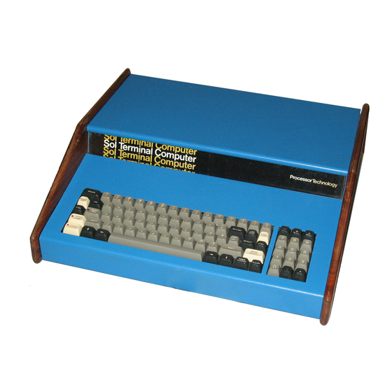
- Page 7 We suggest test and use the Sol-PC Single Board Terminal Computer. that you first scan the entire manual before starting assembly. Then make sure you have all the parts and components listed in the "Parts List"...
- Page 8 Then in- spect the contents for damage. (We suggest you save the shipping materials for use in returning the kit to Processor Technology should it become necessary to do so.) If your Sol-PC kit is damaged, please write us at once describing the condition so that we can take appropriate action.
- Page 9 Sol-PC SINGLE BOARD TERMINAL COMPUTERTM SECTION I 1.2.5 Factory Service In addition to in-warranty service, Processor Technology also provides factory repair service on out-of-warranty Processor Technol- ogy products. Before returning the unit to us, first obtain our authorization to do so by writing us a letter describing the problem.
- Page 10 Sol POWER SUPPLY ASSEMBLY and TEST Introduction ....II-1 Parts and Components ... . II-1 2.2.1 Sol Regulator (Sol-REG) .
- Page 11 PROCESSOR TECHNOLOGY CORPORATION SECTION II Sol POWER SUPPLY INTRODUCTION The Sol power supply consists of a regulator board plus ad- ditional chassis-mounted components. This section covers assembly and test of the complete power supply. PARTS AND COMPONENTS 2.2.1 Sol Regulator (Sol-REG) Check all parts and components against the appropriate "Parts List", Tables 2-1, 2-2 and 2-3.
- Page 12 PROCESSOR TECHNOLOGY CORPORATION Sol POWER SUPPLY SECTION II Table 2-1. Sol Regulator Parts List. INTEGRATED CIRCUITS** DIODES and RECTIFIERS 1458 (U2) MDA101A (FWB2) 7812 (U1) MDA970-1 (FWB1) 7912 (U3) IR106B2 or MCR106-2 (SCR1) 2 1N4001 (D3 & 4) TRANSISTORS 1 1N4148 (D2) 1N5231B (D1) 2 2N2222 (Q2 &...
- Page 13 PROCESSOR TECHNOLOGY CORPORATION SECTION II Sol POWER SUPPLY Table 2-1. Sol Regulator Parts List (Continued). MISCELLANEOUS 1 Sol REG Circuit Board 1 Heat Sink, 690-220-P 1 Heat Sink, 203-AP 1 Heat Sink, aluminum 1 Package Heat Sink Compound 2 Coax Connector, female* (Video Output) 1 Coax Connector, male (Video Output Cable) 1 Coax Connector Adapter Sleeve (Video Output Cable) 1 *AC Receptacle, female...
- Page 14 PROCESSOR TECHNOLOGY CORPORATION SECTION II Sol POWER SUPPLY Table 2-2. Sol-10 Power Supply Parts List. The Sol-10 Power Supply Kit includes all Sol-REG parts listed in Table 2-l plus the following components: 1 *Power Transformer, T1 1 *Fuse, 3 amp Slo-Blo (F1) *Chassis-mounted component Table 2-3.
- Page 15 PROCESSOR TECHNOLOGY CORPORATION SECTION II Sol POWER SUPPLY ASSEMBLY TIPS 2.3.1 Electrical For the most part the assembly tips given in Paragraph 3.2 of Section III (Page III-l) apply to assembling the Sol regulator board and power supply. In addition, scan Section II completely before you start to assemble the power supply.
- Page 16 PROCESSOR TECHNOLOGY CORPORATION SECTION II Sol POWER SUPPLY out of the hole, which may then be applied with a toothpick or small Spread a thin film of the compound on the mating screwdriver blade. surfaces of both the heat-generating component and the heat sink Then assemble as directed.
-
Page 17: Sol-20 Fan Closure Plate Assembly
PROCESSOR TECHNOLOGY CORPORATION Sol POWER SUPPLY SECTION II 2.7.1 Fan Closure Plate Assembly Refer to Assembly Drawings dn Pages X-1 and 2 in Section X. (Figure 2—1 shows a completed fan closure plate assembly.) Figure 2—1. Sol-20 fan closure plate assembly. - Page 18 Prepare RG59/U coaxial cable. Step 7. Cut a 13" piece of coaxial cable from that supplied with the Sol-PC kit. Strip away one inch of the outer insulation at both ends to expose shield. Unbraid shield at one end and twist it into a single lead.
- Page 19 PROCESSOR TECHNOLOGY CORPORATION SECTION II Sol POWER SUPPLY Coaxial cable preparation. Figure 2-2. Connect coaxial cable to coaxial connector in- ( ) Step 8. stalled in Step 6. Solder inner conductor on one end to the pin of the connec- Remove hex nut on upper connector mounting Screw tor.
- Page 20 (shorts) between traces, broken traces and similar defects. If visual inspection reveals any defects, return the board If the board is to Processor Technology for replacement. not defective, proceed to next paragraph. Step 11. Install the following resistors in the indicated locations.
- Page 21 PROCESSOR TECHNOLOGY CORPORATION SECTION II Sol POWER SUPPLY NOTE Disc capacitor leads are usually coated with wax during the manufacturing pro- After inserting leads through cess. mounting holes, remove capacitor and Reinsert clear the holes of' any wax. and install. ORIENTATION LOCATION VALUE (ufd)
-
Page 22: Aluminum Heat Sink Installation
PROCESSOR TECHNOLOGY CORPORATION Sol POWER SUPPLY SECTION II further from the body than the other two leads. Bend leads so that no contact is made with the heat sink when Ul is flat against the sink and its mounting hole is aligned with the holes in the sink and PC board. - Page 23 PROCESSOR TECHNOLOGY CORPORATION SECTION II Sol POWER SUPPLY ( ) Position Q1 (TIP41), with component nomenclature up, on heat sink so hole in Q1 package is aligned with the holes in sink and PC board. Observe how the leads of Q1 must be bent down to fit the pads for Q1 and bend them accord- ingly.
- Page 24 ( ) Twist the two yellow wires together for their full length. *( ) Twist the two blue wires together for their full length. Connect Sol-PC power cable (4-wire cable which Step 26. Tin ends of cable connects to J10 on Sol-PC) to Sol-REG.
-
Page 25: Sol-10 Power Supply Subchassis Assembly
PROCESSOR TECHNOLOGY CORPORATION Sol POWER SUPPLY SECTION II Step 30. Place #4 lockwashers on two 4-40 x 3/16 binder or pan head screws. Insert these screws from the bottom side of the power supply subchassis through the two mounting holes located near the middle of the bottom of the power supply subchassis, one on each side. - Page 26 PROCESSOR TECHNOLOGY CORPORATION Sol POWER SUPPLY SECTION II Position FWB3 (MDA980-l) on power supply subchassis as shown in drawing on Page X-2. BE SURE NEGATIVE (-) TERMINAL OF FWB3 is next to transformer. Insert a 6—32 x. ½ binder or pan head screw from bottom of subchassis, place #6 lockwasher on screw and secure with 6—32 hex nut.
- Page 27 Place #6 lockwasher on each screw and secure with 6-32 hex nut. (Refer to Figure 2-4.) ( ) Step 37. Route Sol-PC power cable between C8 mounting ring and the transformer, mount C8 in its mounting ring, and (See Figure 2-4.) tiqhten clamping-screw.
- Page 28 Install fuse in fuse holder. CAUTION: REMOVE FUSE WITH POWER ON. Check connector on Sol-PC power cable (4 wire) to insure it is wired as shown in Figure 2-6. Check connector on Sol-20 power cable (5 wire) to insure it is wired as shown in Figure 2-7.
-
Page 29: Sol-Pc Power Connector And Voltage Measurements
White/Yellow Green - - - - - -12 V dc (+ .6 v) < White (Ground) ----- Figure 2-6. Sol-PC power connector and voltage measurements. Yellow/White Red/White Blue White (Gnd 1) White (Gnd ----- Figure 2-7. Sol-20 power connector and voltage measurements. - Page 30 III-7 Orientation (Sol-PCB) ... III-7 Sol-PC Assembly-Test Procedure ..III-7 3.6.1 Circuit Board Check ..III-8 3.6.2...
- Page 31 ASSEMBLY TIPS Scan Sections III and IV in their entirety before you start to assemble your Sol-PC kit. In assembling your Sol-PC, you will be following an in- tegrated assembly-test procedure. Such a procedure is designed to progressively insure that individual circuits and sections in the Sol-PC are operating correctly.
- Page 32 PROCESSOR TECHNOLOGY CORPORATION Sol-PC SINGLE BOARD TERMINAL COMPUTER SECTION III Table 3-1. Sol-PC Parts List. INTEGRATED CIRCUITS AM0026 or DMO026 (U104) 74S04 (U92) 7406 (U57,87) 4N26 (U39) 74LS10 (U47,61) 8T94 (U58) 74LS20 (U23,59,83) 8T97 (U67,68,77,80,81) 74LS86 (U74) 1458CP or 1558CP (U56,108)
- Page 33 PROCESSOR TECHNOLOGY CORPORATION 501-PC SINGLE BOARD TERMINAL COMPUTER (Continued) SECTION III Table 3-1. Sd—PC Parts List (Continued). RESISTORS CAPACI TORS ohm, ½ watt, 5% pfd, disc ohm, ¼ watt, 5% pfd, disc ohm, ¼ watt, 5% pfd, disc 1 100 ohm, ¼...
- Page 34 PROCESSOR TECHNOLOGY CORPORATION Sol-PC SINGLE BOARD TERMINAL COMPUTER SECTION III Table 3-1. Sal—PC Parts List (Continued). MISCELLANEOUS 1 Sol—PCB Circuit Board length of #24 bare wire 2 8-pin DIP Socket 29 14-pin DIP Socket 74 16-pin DIP Socket 1 24-pin DIP Socket...
- Page 36 SECTION III ASSEMBLY PRECAUTIONS 3.3.1 Handling MOS Integrated Circuits Many of the IC's used in the Sol-PC are MOS devices. They can IC's be damaged by static electricity discharge. Always handle MOS so that no discharqe will flow throuqh the IC.
- Page 37 Sol-PCB assume this orientation. Sol-PC ASSEMBLY-TEST PROCEDURE The Sol-PC is assembled and tested in sections and/or cir- cuits. You will first test the Sol-PCB circuit board for shorts (solder bridges) between the power buses and After ground.
- Page 38 -12-volt bus are not shorted to each other or to ground. Using an ohmmeter, on "OHMS X 1K" or "OHMS X 10K" scale, make the following measurements (refer to Sol-PC Assembly Drawing X-3). +5-volt Bus Test. Measure between positive and neg- ative mounting pads for C58.
- Page 39 If you wish to wait to assemble the personality module until it is needed, go on to Paragraph 3.6.3. Sol-PCB Assembly and Test 3.6.3 Refer to Sol-PC assembly drawing X-3. Step 1. Install DIP sockets. Install each socket in the in- dicated location with its end notch oriented as shown on the circuit board and assembly drawinq.
- Page 40 PROCESSOR TECHNOLOGY CORPORATION Sol-PC SINGLE BOARD TERMINAL COMPUTER SECTION III LOCATION TYPE SOCKET ( ) U62 through 68 16 pin ( ) U69 40 pin ( ) U70 through 73 16 pin ( ) U74 14 pin ( ) U75 through 81...
- Page 41 PROCESSOR TECHISIOLOGY CORPORATION Sol-PC SINGLE BOARD TERMINAL COMPUTER TM SECTION III LOCATION VALUE (ufd) TYPE ORIENTATION .047 Disc None .047 “ “ .047 “ “ .047 “ “ Tantalum “+” lead bottom .047 Disc None Step 3. Check for +5-volt bus to ground shorts. Using an ohmmeter, measure between positive and negative mounting pads for C58.
- Page 42 PROCESSOR TECHNOLOGY CORPORATION Sol-PC SINGLE BOARD TERMINAL COMPUTER SECTION III LOCATION VALUE (ufd) TYPE ORIENTATION .047 Disc None .047 “ “ .047 “ “ .047 “ “ .047 “ “ .047 “ “ .047 “ “ .047 “ “ .047 “...
- Page 43 PROCESSOR TECHNOLOGY CORPORATION Sol-PC SINGLE BOARD TERMINAL COMPUTER SECTION III LOCATION VALUE TYPE Disc Monolythic or Disc Monolythic or Disc .001 ufd Disc Monolythic Disc Disc Step 11. Install 14.318 MHz crystal in its location just above C61. Insert leads and pull down until the case is 1/16"...
- Page 44 PROCESSOR TECHNOLOGY CORPORATION Sol-PC SINGLE BOARD TERMINAL COMPUTER SECTION III CAUTION 1 NEVER CONNECT POWER CABLE TO J10 WITH POWER SUPPLY ENERGIZED. CAUTION 2 MAKE SURE POWER CABLE CONNECTOR MATES EXACTLY WITH J10; THAT IS, PIN 1 TO PIN 1, PIN 2 TO PIN 2, ETC. ANY OTHER MATING RELATIONSHIP WILL “BLOW”...
-
Page 45: Clock Circuit Waveforms
PROCESSOR TECHNOLOGY CORPORATION Sol-PC SINGLE BOARD TERMINAL COMPUTER SECTION III CHECK POINT SIGNAL WAVEFORM 14.3 MHz square wave. (This is not a U77, Oscillator perfect square wave. It in fact more Pin 7 Output resembles a poor sine wave.) U91,... -
Page 46: Test Probe For Steps 16B And 25B
PROCESSOR TECHNOLOGY CORPORATION Sol-PC SINGLE BOARD TERMINAL COMPUTER TM SECTION III Figure 3-3. Test probe for Steps 16B and 25B. NOTE 1 The probe shown in Figure 3-3 can be made using parts supplied with your Sol-PC kit. Since these parts will... - Page 47 PROCESSOR TECHJWLOGY CORPORATION Sol-PC SINGLE BOARD TERMINAL COMPUTER SECTION III Step 17. Install the following resistors in the indicated locations. Bend leads to fit distance between mounting holes, insert leads, pull down snug to board, solder and trim. LOCATION VALUE (ohms) COLOR CODE 1.5K...
- Page 48 PROCESSOR TECHNOLOGY CORPORATION Sol-PC SINGLE BOARD TERMINAL COMPUTER SECTION III ( ) Step 18. Install the following capacitors in the indicated locations. Take care to observe the proper value and type for each installation. Bend leads outward on solder (back) side of board, solder and trim.
-
Page 49: Coaxial Cable Preparation
PROCESSOR TECHNOLOGY CORPORATION SECTION III Sol-PC SINGLE BOARD TERMINAL COMPUTER Outer Insulation Inner Conduct0 Coaxial cable preparation. Figure 3-4. ( ) Insert twisted shield in mounting hole P2, solder and trim. Using the two large holes to the right of VR1 and VR2, tie cable to board with tie wrap (see CAUTION below). - Page 50 ( ) Turn off power supply and disconnect power connector. ( ) Step 26. Check synchronization circuits. ( ) Set all S1 switches to OFF. ( ) Connect Sol-PC video output cable to video monitor. SEE CAUTION ON PAGE III-22 BEFORE CONNECTING MONITOR. (Step 26 continued on Page 111-22.)
-
Page 51: Display Section Timing Waveforms
PROCESSOR TECHNOLOGY CORPORATION SECTION III Sol-PC SINGLE BOARD TERMINAL COMPUTER WAVEFORM CHECK POINT ( ) U28, Pin 12 6 0 0 ( ) U47, Pin 8 64 us > 5 5 0 n s ( ) U59, Pin8 ( ) U43,Pin9... - Page 52 TO A MONITOR OR TV RECEIVER THAT IS NOT EQUIPPED WITH AN ISOLATION TRANSFORMER. (SEE PAGE AVI-7 IN APPENDIX VI.) ( ) Set VR2 (VERT) and VR1 (HORIZ) on the Sol-PC to their mid- Turn monitor on and apply power to the range settings.
-
Page 53: Bending Selected Pins On U42, 59 And 75
PROCESSOR TECHNOLOGY CORPORATION Sol-PC SINGLE BOARD TERMINAL COMPUTER SECTION III IC NO. TYPE ( ) U1* 4029* ( ) U2 74L5175 25L5175 ( ) U1l* 4029* ( ) U12 74L5157 ( ) U13 74L5175 25L5175 ( ) U25* MCM6574 MCM6575*... - Page 54 Pin l2 to l6 Figure 3-7. U14 through U21 socket jumpers. Turn monitor on and apply power to Sol-PC. Momentarily ground pin 1 of U2 and pin 5 of U75. The display shown in Figure 3-8 should appear on the monitor screen.
-
Page 55: Display Circuits Test Pattern
PROCESSOR TECHNOLOGY CORPORATION Sol-PC SINGLE BOARD TERMINAL COMPUTER SECTION III Figure 3-8. Display circuits test pattern with 6575 character generator as U25. 6574 is the same except graphic control charac- ters are displayed. Step 29. Install 91LO2APC or 21O2L1PC IC’s in locations U14 through U21. - Page 56 PROCESSOR TECHNOLOGY CORPORATION Sol-PC SINGLE BOARD TERMINAL COMPUTER SECTION III LOCATION VALUE (ohms) COLOR CODE 1.5K brown-green-red 1.5K “ “ “ 1.5K “ “ “ 1.5K “ “ “ 1.5K “ “ “ 1.5K “ “ “ 1.5K “ “...
- Page 57 74LS109 74LS109 8T97 8T97 74LS175 74LS367 U107 74LS367 ( ) Step 36. Apply power to Sol-PC and make the following voltage measurements: MEASUREMENT POINT VOLTAGE* Pin 11 of U105 Socket V dc +- .25v Pin 20 of U105 Socket V dc +- .25v Pin 28 of U105 Socket +12 V dc +- .6 V...
- Page 58 ( ) If the test fails, determine and correct the cause before proceeding with assembly. ( ) If the Sol-PC passes this test, turn monitor and power off, disconnect power cable and proceed to Step 39. supply...
-
Page 59: Cpu Functional Test No. 1 Display
( )If the test fails, determine and correct the cause be- fore proceeding with assembly. ( )If the Sol-PC passes this test, turn monitor and power supply off, disconnect power cable and proceed to Step 41. Rev A... - Page 60 74LS175 ( ) U70 74LS109 Step 42. Turn monitor on, apply power to Sol-PC and perform the test described in Step 40, except ground ~in S of U75 in- stead of pin 2. You should get the same results. ( )If the test fails, determine and correct the cause before proceeding with assembly.
-
Page 61: Cpu Functional Test No. 2 Display
PROCESSOR TECHNOLOGY CORPORATION SECTION III Sol-PC SINGLE BOARD TERMINAL COMPUTER Using four 4-40 x 1/4 binder head screws, lockwashers ( ) Step 45. and hex nuts, install two brackets (Sol-1040) for personality Position brackets over the module in area to right of J5. - Page 62 ( ) Step 48. Test memory and decoder circuits. ( ) Set Sl switches as specified in Step 38. ( ) Turn monitor on and apply power to Sol-PC. ( ) Ground pin 1 of U2. You should see the same display as shown in Figure 3-10 on Page III—31.
-
Page 63: Assembly
PROCESSOR TECI~OLOGY CORPORATION Sal-PC SINGLE BOARD TERMINAL COMPUTER SECTION III If the test fails, determine and correct the cause before proceeding with assembly. If the Sol—PC passes this test, turn monitor and power supply off, disconnect power cable, set Switch No. 1 of S1 to OFF and go on to Step 49. - Page 64 PROCESSOR TECHNOLOGY CORPORATION Sol-PC SINGLE BOARD TERMINAL COMPUTER SECTION III LOCATION VALUE (obms) COLOR CODE ( ) R72 blue-gray-brown ( ) R73 ” ” ” ( ) R74 ” ” ” ( ) R75 ” ” ” ( ) R76 ”...
- Page 65 PROCESSOR TECHNOLOGY CORPORATION Sol-PC SINGLE BOARD TERMINAL COMPUTER TM SECTION III Step 5.6. Using two 4-40 x 7/16 binder head screws1 hex nuts and lockwashers, install 25—pin male connector in location J2 (parallel I/O interface). Install J2 in the same manner as you did Jl.
- Page 66 Connect Sol—PC video output cable to monitor, turn moni- tor on and apply power to Sol-PC. Set Sol-PC to local by depressing LOCAL key on keyboard to turn keyboard indicator light on. Data entered from the keyboard should appear on the monitor.
- Page 67 PROCESSOR TECHNOLOGY CORPORATION Sol-PC SINGLE BOARD TERMINAL COMPUTER SECTION III Step 61. Install the following capacitors in the indicated locations. Take care to observe the proper value and type for each installation. Bend leads outward on solder (back) side of board, solder and trim. (Refer to NOTE in Step 2.)
- Page 68 PROCESSOR TECHNOLOGY CORPORATION Sol-PC SINGLE BOARD TERMINAL COMPUTER TM SECTION III Step 66. Install diodes Dl3 and Dl4 (lN400l) in their loca- tions in the lower right corner of the board. Position both diodes with their dark band (cathode) at the bottom.
- Page 69 PROCESSOR TECHNOLOGY CORPORATION Sol-PC SINGLE BOARD TERMINAL COMPUTER TM SECTION III Measure the DC voltage at pin 13 of UllO and write the measured voltage down. (Call this Voltage B.) Add Voltages A and B and divide the sum by 2. (Call the result Voltage C.) An example follows:...
- Page 70 PROCESSOR TECHNOLOGY CORPORATION Sal-PC SINGLE BOARD TERMINAL COMPUTER SECTION III 3.6.4 Modification for 625 Line Video The European televisions standard defines a raster of 625 lines at a field rate of 50 Hz. The horizontal rate of the U.S. standard, 15,750 Hz., is maintained. Only the number of scan lines on the screen is increased.
- Page 71 PERSONALITY MODULE ASSEMBLY Parts and Components ... . IV-1 Assembly Tips ....IV-1 Assembly Precautions ... . IV-1 Required Tools, Equipment and Materials IV-1...
- Page 72 PROCESSOR TECHNOLOGY CORPORATION Sol PERSONALITY MODULE SECTION IV PARTS AND COMPONENTS When ordering your Sol, you selected one of two types of Per- sonality Modules: CONSOL Or SOLOS. The outer carton of your kit is stamped with the Personality Module type. Both use the same PC board marked 2708, assembly #107000, and differ only in the type of ROM’s...
- Page 73 12. There should be no continuity in any of these measurements. If visual inspection reveals any defect, or you measure continuity in any of the preceding tests, return the board to Processor Technology for replacement. If the board is not defective, proceed to next paragraph. 4.6.2 Assembly-Test Procedure Refer to personality module assembly drawing X-6.
- Page 74 PROCESSOR TECHNOLOGY CORPORATION Sol PERSONALITY MODULE SECTION IV DAMAGED BY SIATIC ELECTRICITY DISCHARGE. HANDLE THESE IC’s SO THAT NO DISCHARGE FLOWS THROUGH THE IC. AVOID UNNECESSARY HANDLING AND WEAR COTTON, RATHER THAN SYNTHETIC, CLOTHING WHEN HANDLING MOS IC’s. (STATIC DISCHARGE PROBLEMS ARE MUCH WORSE IN LOW HUMIDITY CONDITIONS.)
- Page 75 PROCESSOR TECHNOLOGY CORPORATION Sol PERSONALITY MODULE SECTION IV LOCATION VALUE COLOR CODE ( ) R1* 100 ohms brown—black—brown ( ) R2* 100 ohms brown-black-brown ( ) R3 brown-black-orange ( ) R4* brown-black-orange ( ) R5 brown-black-orange ( ) R6 brown—black—orange...
- Page 76 (solder) side of the board, cut the trace which connects these pads. Step 8. Stop assembly at this point and proceed with Sol-PC assembly and test up through Step 48. (See Section III.) Then go on to Step 9 of this procedure.
- Page 77 ( ) U3 74LS08 *MOS devices. See CAUTION on pages IV-2, 3. Step 11. Plug personality module into J5 on Sol-PC and con- nect Sol-PC video output cable to video monitor. (Refer to CAUTION on Page III-22 in Section III.) ( ) Set S1 switches as follows: No.
- Page 78 PROCESSOR TECHNOLOGY CORPORATION Sol PERSONALITY MODULE SECTION IV If a blinking cursor is present, the ENter and DUmp commands should operate as described in Section IX of this manual. If the ENter and Dump commands do not operate cor- rectly, locate and correct the problem before pro- ceeding.
- Page 79 KEYBOARD ASSEMBLY and TEST Parts and Components ... . Assembly Tips ....Assembly Precautions ... . Required Tools, Equipment and Materials Orientation .
- Page 80 PROCESSOR TECHNOLOGY CORPORATION Sol KEYBOARD SECTION V PARTS AND COMPONENTS Check all parts and components against the “Parts List”, Table 5-1. If you have difficulty in identifying any parts by sight, refer to Figure 3—1 on Page Ill—S in Section III of this manual.
- Page 81 PROCESSOR TECHNOLOGY CORPORATION Sol KEYBOARD SECTION V Table 5—I. Sol Keyboard Parts List. INTEGRATED CIRCUITS 555 (U3) 74LS30 (U25) 2101 or 9101 (U20) 7442 (U17 & 21) 4051A (U19 & 22) 74LS74 (U8,9,ll,l5,26) 74LS00 (U4,10,14,16) 7493 (U6,U5) 74LS04 (U23) 74LSI32 (U7)
- Page 82 There should be no continuity. If no visual inspection reveals any defect, or you measure continuity between the GND and +5v pads, return the board to Processor Technology for replacement. If the board is not defective, proceed to next paragraph. 5.6.2 Assembly-Test Procedure Refer to keyboard assembly drawing X-7.
- Page 83 PROCESSOR TECHNOLOGY CORPORATION Sol KEYBOARD SECTION V CAUTION SOME MOS INTEGRATED CIRCUITS ARE USED ON THE Sol KEYBOARD. THEY CAN BE DAMAGED BY STATIC ELECTRICITY DISCHARGE. HANDLE MOS IC’s SO THAT NO DISCHARGE FLOWS THROUGH TEE IC. AVOID UNNECESSARY HANDL- ING AND WEAR COTTON, RATHER THAN SYNTHE- TIC, CLOTHING WHEN YOU DO HANDLE MOS IC’s.
- Page 84 PROCESSOR TECHNOLOGY CORPORATION Sal KEYBOARD SECTION V LOCATION VALUE TYPE ORIENTATION Disc None .047 “ “ .047 “ “ .0022 ufd “ “ “ “ “ “ “ “ “ “ .047 “ “ .047 “ “ Tantalum “+” lead top Step 3.
- Page 85 PROCESSOR TECHNOLOGY CORPORATION Sol KEYBOARD SECTION V LOCATION VALUE (ohms) COLOR CODE 1.5K brown—green—red 1.5K “ “ “ blue-gray-orange 1.5K brown—green-red 2.2K red-red-red Step 4. Install Zener diode D1 (1N5221B) in its location to the left of R17. Position Dl with its dark band (cathode) at the bottom.
- Page 86 Step 11. Connect 20-conductor ribbon cable between J1 on keyboard to J3 on Sol—PC so that cable goes left from J3. Step 12. Check keyboard operation. Set S1 switches on Sol-PC as follows: No. 1 through 4: No. 5: No. 6:...
- Page 87 Sol-PC power off, disconnect 20—conductor ribbon cable at Jl on the keyboard and go on to Step 13. Step 13. Place keyboard assembly carefully over key pads on PC board.
- Page 88 It is now ready for use with the Sol—PC Single Board Terminal Computer TM Having completed the Sol keyboard, power supply, Sol-PC and person- ality module, you are now ready to assemble the Sol cabinet—chassis.
- Page 109 Sol operating controls are identified and their functions briefly defined in Table 7-1 on Page VII-2. Unless noted otherwise, the location of each control is shown on the Sol-PC assembly drawing in Section X, Page X-3. BASIC OPERATING MODES 7.3.1...
- Page 110 PROCESSOR TECHNOLOGY CORPORATION Sol OPERATING PROCEDURES SECTION VII Table 7-1. Sol Operating Controls and Their Functions. CONTROL FUNCTION ON-OFF Switch Connects and disconnects primary power to Sol. (See Figure 7-1) RST (Restart) Permits manual restart of Sol without turning Switch, S1-1 power off.
- Page 111 PROCESSOR TECHNOLOGY CORPORATION Sol OPERATING PROCEDURES SECTION VII The command mode allows the introduction of the second level of software. This level includes higher-level language programs such as BASIC/5 or FOCAL in which complex application programs may be more easily written.
- Page 112 7.4.1 Monitor and Cassette Recorder Connections The basic Sol system consists of the Sol, a video monitor for display (e.g., the Processor Technology PT-872 TV-Video Monitor by Panasonic) and a cassette recorder for external storage (e.g., the Panasonic Model RQ-413S).
- Page 113 PROCESSOR TECHNOLOGY CORPORATION Sol OPERATING PROCEDURES SECTION VII ( ) Step 1. Remove top and keyboard covers from Sol. ( ) Step 2. Plug one end of Audio In Cable into Audio IN jack (J7) on Sol rear panel, and plug other end into MONITOR or EARPHONE jack on recorder.
- Page 114 PROCESSOR TECHNOLOGY CORPORATION Sol OPERATING PROCEDURES SECTION VII Figure 7-1. Connecting the basic Sol system VII-6...
- Page 115 PROCESSOR TECHNOLOGY CORPORATION Sol OPERATING PROCEDURES SECTION VII 1 2 3 4 5 6 7 8 1 2 3 4 5 6 7 8 1 2 3 4 5 6 REAR OF Sol 6 5 4 3 2 1 FRONT OF Sol FRONT OF Sol Figure 7-2.
- Page 116 PROCESSOR TECHNOLOGY CORPORATION Sol OPERATING PROCEDURES SECTION VII ( ) Step 8. Turn Sol and monitor on. ( ) Step 9. If the monitor display raster is out of sync (black horizontal bar moves slowly down screen, numerous black lines cut across raster, or both), adjust monitor vertical and horizontal hold controls for a stable raster.
- Page 117 PROCESSOR TECHNOLOGY CORPORATION Sol OPERATING PROCEDURES SECTION VII NOTE: All commands must be given in upper case characters in order to be recognized, and the RETURN key must be pressed after a command so that SOLOS can execute the command (MODE SELECT excepted).
- Page 118 PROCESSOR TECHNOLOGY CORPORATION Sol OPERATING PROCEDURES SECTION VII to the serial channel input and then displayed on the video monitor. You have consequently just "tested" the CPU, serial channel and display section functions in your Sol. 7.4.3 Command Mode Operation The following operations assume your Sol is equipped with a SOLOS personality module.
- Page 119 PROCESSOR TECHNOLOGY CORPORATION Sol OPERATING PROCEDURES SECTION VII ( ) Step 25. Type the XEQ command as follows: XEQ BASIC ( ) Step 26. Press the RETURN key on Sol. The cursor should disappear and the tape should advance. The display should not change otherwise.
- Page 120 (ACI) and the Sol RAM. You have consequently just tested the functions of these sections. OPERATING CONTROLS IN DEPTH Unless indicated otherwise, the location of the controls described in this paragraph are shown on the Sol-PC assembly drawing in Section X, Page X-3. VII-12...
- Page 121 PROCESSOR TECHNOLOGY CORPORATION Sol OPERATING PROCEDURES SECTION VII 7.5.1 ON-OFF Switch (See Figure 7-1 on page VII-6.) Push this switch in to turn your Sol on. In the ON position the switch remains locked in its "in" position. To turn your Sol off, push the switch again.
- Page 122 PROCESSOR TECHNOLOGY CORPORATION Sol OPERATING PROCEDURES SECTION VII S2-1 is the least significant data bit (D100) and S2-8 is the most significant data bit (DIO7). To pull a DIO bit low (when the program tests SSW0 - 7), set the switch associated with the bit to ON.
- Page 123 ***Assumes K-to-M jumper on Sol-PC is not installed. With K-M jumper in and L-M trace on back side of Sol-PC cut, SDI operates at 9600 Baud when S3-8 is ON and all others OFF. NOTE FOR REV D Sol-PC BOARDS:...
- Page 124 PROCESSOR TECHNOLOGY CORPORATION Sol OPERATING PROCEDURES SECTION VII display on the monitor. Use this type of operation when your Sol works with an external computer that does not "echo" data back to the Sol. For full duplex: operation in the terminal mode, set S4-6 to OFF.
- Page 125 PROCESSOR TECHNOLOGY CORPORATION Sol OPERATING PROCEDURES SECTION VII INDIVIDUAL KEY DESCRIPTIONS The exact function of most keys on the Sol keyboard is determined by the software used (e.g., the personality module). Others have predefined functions that are common to the CONSOL and SOLOS Personality Modules.
- Page 126 PROCESSOR TECHNOLOGY CORPORATION Sol OPERATING PROCEDURES SECTION VII Table 7-4. Sol Keyboard Assignments. VII-18...
- Page 127 PROCESSOR TECHNOLOGY CORPORATION Sol OPERATING PROCEDURES SECTION VII Table 7-4. Sol Keyboard Assignments. (Continued) *See notes at end of this table. Page VII-21. VII-19...
- Page 128 PROCESSOR TECHNOLOGY CORPORATION Sol OPERATING PROCEDURES SECTION VII Table 7-4. Sol Keyboard Assignments. (Continued) VII-20...
- Page 129 PROCESSOR TECHNOLOGY CORPORATION Sol OPERATING PROCEDURES SECTION VII HEXADECIMAL CODE/CHARACTER GENERATION UNSHIFTED SHIFTED CONTROL KEY# Symbol Symbol Symbol HEX. HEX. HEX. Displayed* Displayed* Displayed* Code Code Code 6574 6575 6574 6575 6574 6575 SPECIAL KEYS LOAD None None None MODE SELECT...
- Page 130 PROCESSOR TECHNOLOGY CORPORATION Sol OPERATING PROCEDURES SECTION VII 7.7.4 ESCAPE Key Pressing ESCAPE, shifted or unshifted, generates the ASCII escape character (1B). The character is displayed. 7.7.5 BREAK Key Pressing BREAK, shifted or unshifted, forces the SDI output line to a space level for as long as the key is depressed.
- Page 131 PROCESSOR TECHNOLOGY CORPORATION Sol OPERATING PROCEDURES SECTION VII Table 7-5. Control Character Symbols and Definitions. VII-23...
- Page 132 PROCESSOR TECHNOLOGY CORPORATION Sol OPERATING PROCEDURES SECTION VII 7.7.10 LOCAL Key/Indicator The LOCAL key internally connects the SDI output to the SDI input and disables serial transmission. No character is displayed. Pressing LOCAL, shifted or unshifted, to turn the indicator light on sets Sol for local operation.
- Page 133 PROCESSOR TECHNOLOGY CORPORATION Sol OPERATING PROCEDURES SECTION VII 7.7.17 Cursor Control (HOME CURSOR and Arrows) Keys Five keys control basic cursor movement. They are HOME CURSOR and the four keys with arrows. None are affected by SHIFT status, and none are displayed or transmitted.
- Page 134 PROCESSOR TECHNOLOGY CORPORATION Sol OPERATING PROCEDURES SECTION VII If you see the error immediately (the error is to the immediate left of the cursor), press the DEL key (unshifted) to erase the mistake. Then make the correction. If the error is more than one character position to the left of the cursor, use the arrowed cursor control keys to position the cursor over the mistake.
- Page 135 PROCESSOR TECHNOLOGY CORPORATION Sol OPERATING PROCEDURES SECTION VII "monitor" output in the record mode. (Panasonic RQ-413S and RQ-309DS do, for example.) NOTE 1 Recorders on which the "monitor" jack is labeled MONITOR usually provide a monitor output in the record mode.
- Page 136 PROCESSOR TECHNOLOGY CORPORATION Sol OPERATING PROCEDURES SECTION VII RECORDER CONNECTIONS CONNECTIONS CABLING AUXILIARY (J6) Input Audio (Unit 1) AUXILIARY Input Shielded Cable (Unit 2) MONITOR (J7) (Unit 1) Audio MONITOR (Unit 2) (J8) REMOTE Motor (Unit 1) Speaker Wire (J9)
- Page 137 PROCESSOR TECHNOLOGY CORPORATION Sol OPERATING PROCEDURES SECTION VII Set S3 switches to select the Baud rate required by the modem or current loop device. (Standard 8-level TTY's operate at 110 Baud, S3-2 ON and all other S3 switches OFF.) For standard 8-level TTY's and most modems, set all S4 switches OFF.
- Page 138 PROCESSOR TECHNOLOGY CORPORATION Sol OPERATING PROCEDURES SECTION VII CAUTION: PINS 1 AND 2 ON TTY BARRIER STRIP CARRY 120 V ac LINE VOLTAGE. Figure 7-6. Connecting Sol SDI to current loop device such as TTY. *Available at bit 1 of port F8.
- Page 139 PROCESSOR TECHNOLOGY CORPORATION Sol OPERATING PROCEDURES SECTION VII In Figure 7-8, the Oliver OP80 Manual Paper Tape Reader is used to illustrate a typical PDI interconnect. 7.10 CHANGING THE FUSE Sol is protected with a 3.0 amp Slo-Blo fuse housed on the rear panel (see Figure 7-1 on Page VII-6).
- Page 140 INTRODUCTION ....VIII-1 OVERVIEW ..... VIII-1 BLOCK DIAGRAM ANALYSIS, Sol-PC ..VIII-3 8.3.1 Functional Elements And Their Relationships VIII-3 8.3.2...
-
Page 141: Introduction
T.M. Sol Terminal Computer It specifically deals with the operation of the power supply and the logic associated with the Sol-PC and key- board. Descriptions of software and the operation of the circuitry contained in the multitude of integrated circuits (IC's) used in the Sol fall outside the scope of this section. - Page 142 PROCESSOR TECHNOLOGY CORPORATION Sol THEORY OF OPERATION SECTION VIII In the Sol-20, the S-100 Bus structure takes the form of a five-slot backplane board. It consists of a printed circuit board with 100 lines (50 on each side) and five edge connectors on which like-numbered pins are connected from one connector to another.
-
Page 143: Block Diagram Analysis, Sol-Pc
It is also the source of data input to the CPU from eight internal sense switch- es as well as from external memory and I/O. BLOCK DIAGRAM ANALYSIS, Sol-PC 8.3.1 Functional Elements And Their Relationships As can be seen in the Sol block diagram on Page X-24 in Sec- tion X, timing signals for Sol are derived from a crystal controlled oscillator that produces a "dot clock"... - Page 144 PROCESSOR TECHNOLOGY CORPORATION Sol THEORY OF OPERATION SECTION VIII As can be seen, Sol's internal memory consists of four con- tiguous 1024-byte pages. There are two pages (C0 and C4, hexadecimal or hex) of ROM, with Page C0 at hex addresses C000 through C3FF and Page C4 at hex addresses C400 through C7FF.
-
Page 145: Typical System Operation
PROCESSOR TECHNOLOGY CORPORATION Sol THEORY OF OPERATION SECTION VIII Output data from the CPU that is channeled through the Paral- lel Port (PP) is latched from the Bidirectional Data Bus by the par- allel strobe from the Address Page and I/O Port Decoder. -
Page 146: Sdi/Uart Transfer And Display
PROCESSOR TECHNOLOGY CORPORATION Sol THEORY OF OPERATION SECTION VIII done over the Address Bus; cursor position and the "A" enter the Dis- play RAM on the Bidirectional Data Bus.) The CPU is now finished with the transfer, and will issue the next activity command. - Page 147 PROCESSOR TECHNOLOGY CORPORATION Sol THEORY OF OPERATION SECTION VIII Fused primary power is applied through S5 to T1 (T2 in the Sol-20). FWB1, a full-wave bridge rectifier, is connected across the 8-volt secondary (green leads). The rectified output is filtered by C8 and applied to the collector of Q1.
-
Page 148: Sol-Pc Circuit Descriptions
Again, this voltage is supplied to the backplane board in the Sol-20. Sol-20 also includes a cooling fan powered by the AC line voltage. Sol-PC CIRCUIT DESCRIPTIONS 8.5.1 CPU and Bus Refer to the CPU and Bus Schematic in Section X, Page X-15. - Page 149 PROCESSOR TECHNOLOGY CORPORATION Sol THEORY OF OPERATION SECTION VIII Sol is normally configured with the D-to-E jumper installed to meet the clock requirements of the 8080A CPU. With this jumper installed, the outputs of the third and fourth U90 stages are applied to pins 9 and 10 of U91.
- Page 150 φ NAND gate U91. It occurs 70 nsec after It is used on the Sol-PC and is also made available on S-100 Bus pin 49 as a general 2.04, 2.38 or 2.86 MHz clock signal. Three J-K flip-flops (U63 and 64) are used to synchronize the READY, RESET and HOLD inputs to the CPU.
- Page 151 VIII-11...
- Page 152 PROCESSOR TECHNOLOGY CORPORATION Sol THEORY OF OPERATION SECTION VIII Diode D7, Cl5 and R18 make up the POC (power on clear) cir- cuit. When power is applied, Cl5 starts to charge slowly until it reaches the threshold on pin 6 of U46, a Schmitt trigger.
- Page 153 PROCESSOR TECHNOLOGY CORPORATION Sol THEORY OF OPERATION SECTION VIII The inverted DBIN on pin 3 of U46 is also applied to pin 12 of NOR gate U46 and inverted to appear as PDBIN on S-100 Bus pin 78. This section of U46 also allows !DIG1 (bus pin 57) to override DBIN.
-
Page 154: Memory And Decoder
PROCESSOR TECHNOLOGY CORPORATION Sol THEORY OF OPERATION SECTION VIII Input selection to the multiplexers is done with the A and B inputs to U65, 66, 78 and 79. These two inputs are driven by MPX_ ADR_A on pin 3 of NOR gate U48 and MPX_ADR_B on pin II of NOR gate U48. - Page 155 PROCESSOR TECHNOLOGY CORPORATION Sol THEORY OF OPERATION SECTION VIII The System RAM consists of eight 1K by 1 bit static memory chips, U3 through U10, and it is assigned addresses C800-CBFF (hex). When the CPU wants to write data into memory, it addresses the System RAM on ADR0-15.
- Page 156 PROCESSOR TECHNOLOGY CORPORATION Sol THEORY OF OPERATION SECTION VIII The other two enables on U34 (G2A and G2B) are connected to SINP and SOUT. These two status signals indicate an input or output operation during the CPU cycle. U34 is therefore disabled during these operations.
- Page 157 PROCESSOR TECHNOLOGY CORPORATION Sol THEORY OF OPERATION SECTION VIII Table 8-1. Port Decoder (U35 & U36) Outputs and Their Functions. PORT DECODER OUTPUT FUNCTION !PORT_OUT_FE Loads starting row address and first display line position information from Bidirectional Data Bus into Video Display scroll circuit.
-
Page 158: Input/Output
PROCESSOR TECHNOLOGY CORPORATION Sol THEORY OF OPERATION SECTION VIII interrupt operation. To prevent this, SINTA is inverted in U58 to 1) disable U34 on pin 6 and 2) force pin 8 of NAND gate U23 high to dis- able U35 and U36 on pin 5. - Page 159 PROCESSOR TECHNOLOGY CORPORATION Sol THEORY OF OPERATION SECTION VIII PXDR on pin 16 of J2 is supplied by the external device. indicates the device is ready to receive data. !PXDR is buffered to INT2 and will effect the transfer of data to the Internal Data Bus during the status input to the CPU.
- Page 160 (153.6 KHz - 16 = 9600). (The L-M connection is default wired on the Sol-PC; that is, there is a trace between L and M on the circuit board. ) If the L-M trace is cut and a jumper is installed between K and M, the Baud rate with S3-8 is 4800 (76.8 KHz - 16 =...
- Page 161 PROCESSOR TECHNOLOGY CORPORATION Sol THEORY OF OPERATION SECTION VIII Returning to the SDI UART, we see that its transmitter output on pin 25 is applied to pin 5 of U55, a two-input NAND gate that is functionally a NOR gate.
-
Page 162: Display Section
PROCESSOR TECHNOLOGY CORPORATION Sol THEORY OF OPERATION SECTION VIII the light is optically coupled to the base of a photo transistor in U39 to cause the transistor to conduct. Conduction translates to a low, or mark, level at the input (pin 13) of U38. - Page 163 PROCESSOR TECHNOLOGY CORPORATION Sol THEORY OF OPERATION SECTION VIII In the Sol, the display format is 64 characters maximum per character row, with a maximum of 16 rows per frame (page). Thus, up to 1024 characters can be displayed per page.
-
Page 164: Example Of Uppercase Character (I) Display
PROCESSOR TECHNOLOGY CORPORATION Sol THEORY OF OPERATION SECTION VIII SCAN CHARACTER LINE LINE COLUMN NO. ADDRESS* ADDRESS 1 2 3 4 5 6 7 8 9 VIDEO INFORMATION BITS 1001001 1111 O O O O O O O O O 000000000 (blank) ↑... - Page 165 PROCESSOR TECHNOLOGY CORPORATION Sol THEORY OF OPERATION SECTION VIII As indicated in Figure 8-4 on Page VIII-27, Subgroup Counter U31 and Group Counter U33 are preset to a count of 3 at the start of each horizontal scan line. U31 counts from 3 through 15 (13 charac- ter positions) and enables U33 for one count.
- Page 166 PROCESSOR TECHNOLOGY CORPORATION Sol THEORY OF OPERATION SECTION VIII Assume VDISP is active (low), which it is during the vertical display portion of the displayable area on the screen. (Refer to Figure 8-4.) U62 is then preset to a count of 0 and will count from 0 through 15 (16 character rows).
- Page 167 VIII-27...
- Page 168 PROCESSOR TECHNOLOGY CORPORATION Sol THEORY OF OPERATION SECTION VIII The PRE_BLANK input provides "window shade" blanking which is analogous to pulling a window shade down from the top of the display. PRE_BLANK is generated in one half of J-!K flip-flop U43.
- Page 169 PROCESSOR TECHNOLOGY CORPORATION Sol THEORY OF OPERATION SECTION VIII Normally the internal display address is multiplexed to the Display RAM. When the CPU or a DMA device requests access (!PAGE_CC active), the multiplexers switch to the external address lines, ADR0-9.
-
Page 170: 6574 Character Generator Rom Pattern
PROCESSOR TECHNOLOGY CORPORATION Sol THEORY OF OPERATION SECTION VIII Figure 8-5. 6574 Character Generator ROM pattern. "C" and "T" were stored in the RAM in the proper character positions in the third character row. After the first two character rows have been displayed, the... - Page 171 PROCESSOR TECHNOLOGY CORPORATION Sol THEORY OF OPERATION SECTION VIII Figure 8-6. 6575 Character Generator ROM pattern. For the second character position the Character and Line Ad- dress Multiplexers call up the "T" in the Display RAM. The resulting ASCII code for a "T" (1010100) ultimately appears on the address in- puts to the Character Generator ROM.
- Page 172 PROCESSOR TECHNOLOGY CORPORATION Sol THEORY OF OPERATION SECTION VIII Generator ROM automatically outputs all zeros for these two character positions. After the last scan line in the third character row, the Scan Counter is reset to a count of 15 to start the fourth character row.
- Page 173 PROCESSOR TECHNOLOGY CORPORATION Sol THEORY OF OPERATION SECTION VIII set to the outputs of latches U2 and 13. U2 latches the starting row address from DIO0-3 and U13 latches the data on DIO4-7, with !PORT_OUT_FE being the strobe. Data on DIO4-7 specifies where the first line will be displayed.
- Page 174 PROCESSOR TECHNOLOGY CORPORATION Sol THEORY OF OPERATION SECTION VIII the high or low speed clocks. Specifically, A must be high and B low to select high speed clocks; the converse condition selects low speed clocks. The select inputs are supplied by TAPE_HI_SPEED and !TAPE_HI_SPEED.
- Page 175 PROCESSOR TECHNOLOGY CORPORATION Sol THEORY OF OPERATION SECTION VIII respectively, prevent damage to the logic circuitry in the Input/ Output section due to inductive kickback. R155 and 156 are current limiters that keep the relay contacts from "welding" together. When the CDI is in the write mode, data is input to the UART (U69) under control of !PORT_OUT_FB.
- Page 176 PROCESSOR TECHNOLOGY CORPORATION Sol THEORY OF OPERATION SECTION VIII As previously stated, the second stage of U101 is allowed to change state on the positive going transitions of the OUTPUT_CLOCK as long as the data out of the synchronizer is a "1".
- Page 177 PROCESSOR TECHNOLOGY CORPORATION Sol THEORY OF OPERATION SECTION VIII first U108 stage, it serves as a variable shunt. A low gate voltage on Q3 decreases the shunt resistance and the input to U108. In a like manner, a high voltage on C67 results in an increased input to U108.
- Page 178 PROCESSOR TECHNOLOGY CORPORATION Sol THEORY OF OPERATION SECTION VIII U100. The output on pin 12 of U100 is inverted by U109 and applied to the receive input (pin 20) of the UART. The Q output on pin 1 of U113, which occurs at the actual bit rate of the incoming data, is also used by the receive clock cir- cuitry to reconstruct the receive clock from the data signal.
- Page 179 ROM which specify the high order four KBD bits (KBD4-7). All keyboard outputs are supplied to J1 which is connected to J3 on the Sol-PC. 8.6.2 Circuit Description Refer to the Keyboard schematic in Section X, Page X-23.
- Page 180 PROCESSOR TECHNOLOGY CORPORATION Sol THEORY OF OPERATION SECTION VIII !φ 2 respectively. This circuit thus generates a symmetrical two phase clock, with each phase having a 6 usec period with a 1.5 usec nega- tive going pulse. !φ 1 advances the cascaded ripple counter, U5 and 6, in the Column Scanner circuit (U5, U6, NAND gates U4 and decoders U17 and !φ...
- Page 181 PROCESSOR TECHNOLOGY CORPORATION Sol THEORY OF OPERATION SECTION VIII This detector circuit consists of three transistors, Q7, Q8, and Q9 (connected as a linear amplifier with negative feedback) fol- lowed by Q4 and Q2. Q4 and Q2 are large signal amplifiers biased in their cut-off region.
- Page 182 PROCESSOR TECHNOLOGY CORPORATION Sol THEORY OF OPERATION SECTION VIII KEY is fed to pin 5 of 8-input NAND gate U25, pin 9 of ROM U20 and pin 1 of NAND gate U27. Let's examine the other inputs to U25. KEY, as mentioned, is fed to pin 9 of U20 which is a 256 x 4 bit static ROM.
- Page 183 6 is inverted by NAND gate UIO to supply a low active !STROBE on pin 3 of J1. (Note that J1 on the keyboard connects to J3 on the Sol-PC.) The next inverted 6 usec clock resets the second U11 stage.
- Page 184 PROCESSOR TECHNOLOGY CORPORATION Sol THEORY OF OPERATION SECTION VIII following release of KEY. On the third cycle the circuit reverts to its original state. This circuit, comprised of U20, U26, U16 and U17 serves two functions. By requiring two events during two consecutive count cy- cles before generating a KEY, it discriminates against false key clo- sures.
- Page 185 PROCESSOR TECHNOLOGY CORPORATION Sol THEORY OF OPERATION SECTION VIII causes LED3, the LOCAL light, to turn on. A second closure of the LOCAL key toggles this section of U15 to the opposite condition. Note that LOCAL has no affect on keyboard data.
- Page 187 SECTION IX SOFTWARE Sol TERMINAL COMPUTER Processor Technology...
- Page 188 PROCESSOR TECHNOLOGY CORPORATION Sol SOFTWARE SECTION IX CONSOL CONSOL is a 1024 byte program designed to allow the Sol TER- MINAL/COMPUTER to operate as a standard CRT terminal and to provide access to the essential computer capabilities of the Sol.
- Page 189 PROCESSOR TECHNOLOGY CORPORATION Sol SOFTWARE SECTION IX 9.1.1 DUmp (addr) (addr) The DUmp command displays memory data on the screen in a Hexidecimal representation. As with all Sol commands the command is recognized by the first two characters and up to ten additional char- acters can be input without an error being forced.
- Page 190 0 being high speed and 1 being low. (1200 and 300 bits per second respectively). If no parameter is given CONSOL will default to high speed operation as all standard Processor Technology Sol-System Software is recorded at this speed. 9.1.4 EXecute addr The execute command is used to run programs located in ex- ternal memory.
- Page 192 M0100 (tm) (tm) SOLOS /CUTER USER'S MANUAL PROCESSOR TECHNOLOGY CORP. SOFTWARE TECHNOLOGY CORP. 6200 Hollis Street P. O. Box 5260 Emeryville, CA 94608 San Mateo, CA 94402 (415) 652-8080 (415) 349-8080 1977 by Processor Technology Corporation...
- Page 193 I M P O R T A N T N O T I C E This copyrighted software product is distributed on an individual sale basis for the personal use of the original purchaser only. No license is granted herein to copy, duplicate, sell or other- wise distribute to any other person, firm or entity.
- Page 194 SOLOS meaning the SOLOS/CUTER operating system. The few differences between SOLOS and CUTER will be stated explicitly. (tm) SOLOS, CUTER and Sol are trademarks of Processor Technology Corporation.
- Page 195 SOLOS/CUTER User's Manual TABLE OF CONTENTS I. INTRODUCTION Definition of Terms ..Quick Command Reference List ..II. CONSOLE COMMANDS Console Commands in Brief ..Console Commands in Detail Execute Command .
- Page 196 SOLOS/CUTER User's Manual TABLE OF CONTENTS (cont.) SET COMMANDS (cont.) Set CRC Error Checking Command ..Set Number of NULLS Command ..SUBROUTINES Introduction to SOLOS Machine Language Interface .
-
Page 198: Introduction
INTRODUCTION SOLOS is a 2048 byte program that configures the Sol-20 and one or two cassette tape recorders into a powerful, stand-alone computing system. SOLOS takes advantage of the Sol-20's built-in hardware peripherals and the 8080 instruction set to optimize the convenience and power of the inherent computer capabilities of the Sol. -
Page 199: Quick Command Reference List
INTRODUCTION (cont.) Only the first two letters of the command expressions must be typed when entering a command expression. (The underscored letters in the following Quick Command Reference List.) Quick Command Reference List COMMAND FUNCTION Console EXEC addr Begin program execution at 'addr' ENTR addr Enter data into memory starting at 'addr' DUMP addr1 (addr2) - Page 200 INTRODUCTION (cont.) With a Sol, or CUTER on a Processor Technology GPM board, a power- on performs a reset which causes a SOLOS system reset. The Sol user may initiate this system reset anytime by simultaneously pressing the upper case and repeat keys.
-
Page 201: Console Commands
CONSOLE COMMANDS Console Commands in Brief SOLOS has five console commands. They are: Command Function EXEC addr Begin program execution at 'addr'. ENTR addr Enter data into memory starting at 'addr'. DUMP addrl (addr2) Dump memory data, 'addr1' to 'addr2'. TERM (portin (portout)) Enter Terminal Mode (available under SOLOS only) CUST name (addr) -
Page 202: Terminal Command
CONSOLE COMMANDS (cont.) Terminal Command TERM (port-I (port-O)) (Available under SOLOS only) This command causes the Sol system to become a video terminal for connection to an external computer or modem. This command begins by automatically setting the I/O pseudo ports to the specified values. -
Page 203: Tape Commands
III. TAPE COMMANDS Tape commands are used to control the tape cassette recorders. these commands, unit selection is optional, with a default select- ing unit 1. When a unit is specified, however, it must be separated from the file identification name with a slash (/) and without spaces in between: e.g., TARGT/2. -
Page 204: Tape Commands In Detail
III. TAPE COMMANDS (cont.) Tape Commands in Detail Get a file from tape GET (name(/unit) (addr)) This command transfers the specified or next tape file into memory. If a (name/unit) is given, this command will search forward on the cassette until that file is found. The (addr) parameter, if given, specifies the memory location at which the file will be loaded. - Page 205 III. TAPE COMMANDS (cont.) Note: A very useful feature of the CAT command is to apply power to the tape units when needed to rewind tape. Depressing the MODE (or Control-@) key will remove power from tape unit and return to COMMAND mode.
-
Page 206: Set Commands
SET COMMANDS SOLOS has 10 set commands. They are: S=data Screen character rate I=port Input port to SOLOS O=port Output port to SOLOS N=data Number of NULLS following CRLF XEQ addr Auto-execute addr TAPE 0 or 1 0=1200 baud, 1=300 baud TYPE data Type 'byte' header COUT addr... -
Page 207: Set In Command
SET COMMANDS (cont.) The Output Pseudo ports command parameter values are: 0 = Video Display 1 = Serial Output Port 2 = Parallel Output Port 3 = User Defined by SET COUT command Example: SET O=1 DUMP 0 2F Result: Select serial output port. -
Page 208: Set Type Command
SET COMMANDS (cont.) Set Type Command SET TYPE data This command sets (data) values into the 'type' byte in the tape header information when used in conjunction with the SAVE command. The 'type' byte data is entered as a hexadecimal value, but it will appear on the screen as an ASCII character when displayed by the GET or CAT command. -
Page 209: Set Crc Error Checking Command
SET COMMANDS (cont.) Custom Output driver requirements are: The 'addr' (address) word in the SET COUT command will equal the starting address of the output routine. It is the user's responsibility to save registers prior to any modification of the register. The "B"... - Page 210 SET COMMANDS (cont.) initialized to zero but may be set to any number up to FF (hex). This command is useful when using output devices requiring a delay following a carriage return. Example: SET N=3 Result: Every CRLF issued by SOLOS will be followed by three nulls.
-
Page 211: Subroutines
SUBROUTINES Introduction to the SOLOS Machine Language Interface The Machine Language Interface with SOLOS is based on: A predefined set of 'pseudo' I/O ports allowing software compatibility as well as providing an easy means of supporting any I/O device. A system defined register usage when interfacing with SOLOS. -
Page 212: Defined Register Usages
SUBROUTINES (cont.) Second are the defined register usages when interfacing at the machine language level with SOLOS. Whenever a machine program is executed by SOLOS (via the EXEC or XEQ command, or via a custom command), the stack pointer and HL registers are predefined by SOLOS >. -
Page 213: Jump Table
SUBROUTINES (cont.) JUMP TABLE Function Address Label Length This byte allows power-on reset of SOLOS. It C000 START is 00 for SOLOS and 7F for CUTER, providing an easy means of differentiating the exact operating system in use. C001 INIT This is a "JMP"... -
Page 214: System Entry Points
SUBROUTINES (cont.) System Entry Points There are actually only two system entry points within the SOLOS jump table. Entry at these points does not require that any register be initialized. The first (at either label "START" or "INIT") is used to perform a complete power-on system reset. a part of the system reset, the system RAM area data used by SOLOS will be cleared. -
Page 215: Aout
SUBROUTINES (cont.) AOUT entry point address C01C This entry point is used to output one character to any pseudo port. Register "A" is assumed to be a binary value from 0 to 3 indicating the desired output pseudo port. Register "B" will contain the character to be output. return, the PSW and Register "A"... -
Page 216: Cassette Tape Entry Points To Solos
SUBROUTINES (cont.) Escape sequence Function 1B 05 ## 1B 06 ## 1B 07 ## The third byte is output to the VDM at the current cursor position exactly as is, regardless of this byte's value. No check is made of this character (##). -
Page 217: Block Access
SUBROUTINES (cont.) When calling open the register, pair "HL" should point to a memory location that contains the header. Following is the layout of a SOLOS file header: NAME ASC '12345' A five character name with trailing binary zeroes. Should always be zero. TYPE DB 'B'+80H File type. -
Page 218: Write Tape Block Routine
SUBROUTINES (cont.) Registers H & L contain the address of file header information. Registers D & E contain the address-of where the file is to be loaded into memory. (If set to 0, this in- formation is taken from file header information on tape.) On exit: Normal return: Carry Flag is cleared, and data has... -
Page 219: File Open Routine
SUBROUTINES (cont.) SOLOS provides entry points to Open, Read, Write and Close tape files. Each of these routines requires that certain con- ventions be followed to ensure accurate data transfers. File Open Routine FOPEN The Open routine sets up certain internal parameters to keep track of data requests. -
Page 220: Read Byte Routine
SUBROUTINES (cont.) Read Byte Routine RDBYT The Read Byte routine reads a single byte of data from a buffer file. SOLOS fills this buffer as needed per read request. Each time SOLOS fills the file buffer (reads a block), the CRC character is checked for data accuracy. The entry point for RDBYT is C00D. -
Page 221: Loading & Executing Cuter
LOADING & EXECUTING CUTER (Applicable to CUTER only) CUTER is available (1) on cassette tape with its own loader which can be loaded at any memory address from 0200 through F400, or (2) in ROM at the address C000. In order to load CUTER from cassette tape, perform the following steps. - Page 222 LOADING & EXECUTING CUTER (cont.) (Applicable to CUTER only) Via sense switches, select the default I/O pseudo ports as follows: X X X X I I O O 7 6 5 4 3 2 1 0 Where: X X X X doesn't matter which pseudo port from 0 - 3 (00-11 binary) is to be the default input pseudo port.
Need help?
Do you have a question about the Sol-PC and is the answer not in the manual?
Questions and answers