
Summary of Contents for DM&P Group SBC475
- Page 1 Full 16-bit ISA Bus SBC475 DM&P Vortex86DX 800MHz Half-Size CPU Module with 4S/4USB/VGA/LCD/LAN/GPIO/FDD 256MB DDR2 Onboard User’s Manual (Revision 1.1A)
-
Page 2: Table Of Contents
T a b l e C o n t e n t s T a b l e o f C o n t e n t s ............. iii C h a p t e r 1 Introduction……………………………………………1 Packing List ............1 Product Description .......... - Page 3 This page is blank...
-
Page 4: Table O F C O N T E N T S
C h a p t e r Introduction Packing List Product Name Package Embedded Vortex86DX CPU All-in-One Board RS232 cable x 3 SBC475 PRINTER cable x1 IDE cable x 1 FDD cable x 1 USB cable x 2 (USB port x 2 GPIO cable x 1... -
Page 5: Product Description
Half-Size controller. The SBC475 family of controller is designed as a plug in replacement, with backward compatibility to support legacy software to help extend existing product life cycle without heavy re-engineering. -
Page 6: Specifications
1.3 Specifications Features SBC475 DM&P SoC CPU Vortex86DX- 800MHz Real Time Clock with Lithium Battery Backup L1:16K I-Cache, 16K D-Cache L2:128KB Cache Cache AMI BIOS BIOS PC/104 Standard Compliant (Optional: PCI-104) Bus Interface 256 /512MB DDR2 Onboard System Memory Software programmable from 30.5 us to 512 seconds x2... - Page 7 2.54 mm ∅ 26-pin box header for Print x1 Connectors 2.54 mm ∅ 10-pin box header for RS-232 x3 2.54 mm ∅ 10-pin box header for USB x2 2.54 mm ∅ 20-pin box header for 16-bit GPIO x1 2.54 mm ∅ 3-pin header for RS-485 x1 2.54 mm ∅...
-
Page 8: Board Dimension
1.4 Board Dimension Vortex86DX-6324RD-FD Vortex86DX™ Half-Size CPU Module... -
Page 9: Chapter 2 Installation
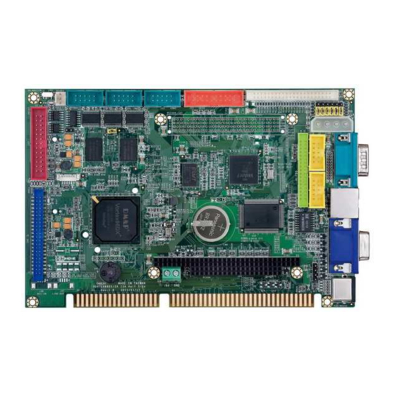
C h a p t e r 2 C h a p t e r 2 C h a p t e r 2 C h a p t e r 2 Installation 2.1 Board Outline COM2 RS-485 RS-232/422/485 Display Type COM4 COM3 GPIO... -
Page 10: Connectors & Jumpers Location
2.2 Connectors & Jumpers Location Connectors... - Page 11 Jumpers & LEDs...
-
Page 12: Connectors & Jumpers Summary
Connectors & Jumpers Summary Summary Table Description Type of Connections Pin nbrs. 44-pin Box Header, 2.0∅ , 22x2 USB1 10-pin Box Header, 2.54∅ , 5x2 USB2 10-pin Box Header, 2.54∅ , 5x2 JTAG 6-pin Wafer, 1.25∅ , 6x1 Reset 2-pin Pin Header, 2,54∅,1x2 Redundancy (Optional) 7-pin... - Page 13 J40 Master/Slave for IDE & CF 3-pin Slide Switch J41 Console Redirection (Optional) 2-pin Pin Header, 2,54∅,1x2 J42 FDD 34-pin Pin Header, 2.0∅ ,17x2 PWR-L Power Active LED (Red) LED-SMD IDE Active LED (Green ) IDE- LED-SMD MTBF- MTBF-Out (Orange) LED-SMD CF1 Compact Flash 50-pin...
-
Page 14: Pin Assignments & Jumper Settings
2.4 Pin Assignments & Jumper Settings J1: IDE (44 Pins) Pin # Signal Name Pin # Signal Name IDERST IDED7 IDED8 IDED6 IDED9 IDED5 IDED10 IDED4 IDED11 IDED3 IDED12 IDED2 IDED13 IDED1 IDED14 IDED0 IDED15 IDEREQ IDEIOW IDEIOR ICHRDY IDEACK IDEINT IDESA1 IDECBLID... - Page 15 J3: USB 2 Pin # Signal Name Pin # Signal Name LUSBD2- LUSBD3- LUSBD2+ LUSBD3+ GGND GGND J4: JTAG (Default setting: off) Pin # Signal Name Pin # Signal Name J5: RESET Pin # Signal Name Pin # Signal Name Reset J6: Redundancy (Optional) Pin #...
- Page 16 J8: PS/2 KBD / Mouse Pin # Signal Name Pin # Signal Name KBCLK MSCLK KBDAT MSDAT GGND GGND GGND J9: COM 1 (Optional: TTL/ GPIO-P4 / PWMx8) Signal Signal Pin # Pin # Name Name DCD1 RXD1 TXD1 DTR1 DSR1 RTS1 CTS1...
- Page 17 J11: GPIO (Port 0 / Port 1/PWMx16) Pin # Signal Name Pin # Signal Name GP00 GP10 GP01 GP11 GP02 GP12 GP03 GP13 GP04 GP14 GP05 GP15 GP06 GP16 GP07 GP17 J12: RS485 (Auto direction) Pin # Signal Name RS485+ RS485-...
- Page 18 J18: Power Connector (Terminal Block 5.0mm) Pin # Signal Name J19: COM3 Pin # Signal Name Pin # Signal Name DCD3 RXD3 TXD3 DTR3 DSR3 RTS3 CTS3 J20: PRINT Pin # Signal Name Pin # Signal Name STB- AFD- ERR- INIT- SLIN- ACK-...
- Page 19 J22: PC/104 Connector – 64pin Pin # Signal Name Pin # Signal Name IOCHCHK RESETDRV IRQ9 DRQ2 -12V +12V IOCHRDY SMEMW * SA19 SMEMR * SA18 IOW * SA17 IOR * SA16 DACK3 * SA15 DRQ3 SA14 DACK1 * SA13 DRQ1 SA12 REFRESH *...
- Page 20 J24: PC/104 Connector – 40pin Pin # Signal Name Pin # Signal Name MEMCS16 * SBHE * IOCS16 * SA23 IRQ10 SA22 IRQ11 SA21 IRQ12 SA20 IRQ15 SA19 IRQ14 SA18 DACK0 * SA17 DRQ0 MEMR * DACK5 * MEMW * DRQ5 DACK6 * DRQ6...
- Page 21 J27: PC/104 + (Optional) VI/O Default setting: +5V If you need to use VI/O as +3.3V, please see the page 19. Pin # AD00 VI/O(+5V) AD02 AD01 AD05 AD04 AD03 C/BE0# AD07 AD06 AD09 AD08 AD11 VI/O(+5V) AD10 AD14 AD13 AD12 +3.3V C/BE1#...
- Page 22 Please remove the R229 and add 0 ohm (1206 type) on R230...
- Page 23 J28: VGA (D-Sub connector) Pin # Signal Name Pin # Signal Name R OUT G OUT B OUT DDCDAT HSYNC VSYNC DDCCLK J29: LCD Connector Pin # Signal Name Pin # Signal Name +3.3V +3.3V LCLK LHSYNC LVSYNC LBACKL LVDDEN (Please refer to Appendix A, for TFT Flat Panel Data Output)
- Page 24 J30~J35: Display type setup (CRT /LCD) Connector Pin # Signal Name GPIOA GPIOB GPIOC GPIOD GPIOE GPIOF (Please refer to Appendix D, for Display type setup) J36: LAN Pin # Signal Name Pin # Signal Name...
- Page 25 J37: LINE OUT (Optional) Pin # Signal Name LOUTR LOUTL J38: MIC-IN (Optional) Pin # Signal Name MICVREF MIC-IN J39: JTAG Disable (Default setting: Pin 1 & Pin 2 short) Pin # Signal Name Pin # Signal Name JTAG Disable J41: Console Redirection (Pin 1 &...
- Page 26 J42: FDD Pin # Signal Name Pin # Signal Name DENSEL INDEX\ MTRO\ DS1\ DS0\ MTR1\ DIR\ STEP\ TR0\ HDSEL\ DSKCHG\...
-
Page 27: System Mapping
System Mapping... -
Page 30: Watchdog Timer
Watchdog Timer There are two watchdog timers in Vortex86SX/DX CPU. One is compatible with M6117D watchdog timer and the other is new. The M6117D compatible watchdog timer is called WDT0 and the new one is called WDT1. We also provide DOS, Linux and WinCE example for your reference. -
Page 31: Gpio
GPIO (General Purpose Input / Output) 40 GPIO pins are provided by the Vortex86SX/DX for general usage in the system. All GPIO pins are independent and can be configured as inputs or outputs, with or without pull-up/pull-down resistors. -
Page 32: Spi Flash
SPI flash (Serial Peripheral Interface) As SPI Flash Serial Peripheral Interface) offers many benefits including: reduced controller pin count, smaller and simpler PCBs, reduced switching noise, less power consumption, and lower system cost Many of users may consider using a formatted SPI flash to boot for the system or emulate SPI flash as Floppy (A: Driver or B: Driver). -
Page 33: Pwm
PWM (Pulse-width modulation) Pulse-width modulation (PWM) of a signal or power source involves the modulation of its duty cycle, to either convey information over a communications channel or control the amount of power sent to a load. The popular applications of pulse width modulation are in speed control of electric motors, volume control of Class D audio amplifiers or brightness control of light sources and many other power electronics applications. -
Page 34: Ide To Sd
IDE to SD (Micro-SD) Vortex86DX SoC also built-in simulation circuit to adapt SD to IDE in order to allow your system to recognize Micro-SD card as C: or D: Driver SD-1917: 44 pins IDE to SD Adapter is an ideal solution for industrial PC or embedded system and 44 pins IDE to SD Adapter can be easily installed on all VDX-63xx CPU boards. -
Page 35: Chapter 3 Driver Installation
Operating system support The SBC475 ISA CPU board provides the VGA and LAN drivers for DOS 6.22 Windows CE 5.0, CE 6.0, Windows 98, Windows XP Professional, Windows Embedded standard (XPE) and Windows 2000. -
Page 36: Appendix
Appendix TFT Flat Panel Data Output Vortex86DX™... -
Page 37: Tft Flat Panel Support List
B.TFT Flat Panel Support List Size Brand Resolution Model No. 5.7” Data image 320x240 FG050701DSSWBG01 5.7” Optrex 320x240 55264GD057J-FW-ABN 5.7” TOSHIBA 320x240 LTA057A343F 5.7” Sharp 320x240 (QVGA / VGA) LQ057Q3DC02 5.7” Kyocera 320x240 (QVGA / VGA) TCG057QV1AC-G10 5.7” 320x240 (QVGA / VGA) PD057VU4 /U5 5.7”... -
Page 38: Lvds Flat Panel Support List
C. LVDS Flat Panel Support List If you would like to use LVDS Flat Panel with Vortex86SX / Vortex86DX series, please contact our regional sales to get SBC475-0096 information or : 18-bit TFT to LVDS converter and Cable-LVDS-30: L VDS Cable 30cm... -
Page 39: Flat Panel Hardware Setting
G121SN01 15” 1024x768 G150XG01 D. Flat Panel Hardware Setting: The SBC475 offers the Hardware setting for t he various TFT LCD Flat Panels support and please make sure the jumper setting (J30~J35) before you connect the LCD. Display type setup Connector Note: "C"... -
Page 40: Flat Panel Wiring And Lighting
E. Flat Panel Wiring and Lighting Hardware Before you connect the TFT LCD Flat Panel with SBC475 ,please make sure that the input Voltage of LCD is 3.3V. BIOS Please contact or e-mail our regional sales to get the special BIOS for any TFT LCD Flat Panels. -
Page 41: Tcp/Ip Library For Dos Real Mode
F. TCP/IP library for DOS real mode DSock is a TCP/IP library for DOS real mode, which is used by RSIP. It provides simple C functions for programmer to write Internet applications. PCW also provide Internet examples using DSock: BOOTP/DHCP, FTP server, SMTP client/server, HTTP server, TELNET server, Talk client/server, etc. -
Page 42: Bios Default Setting
G. BIOS Default setting If the system cannot be booted after BIOS changes are made, Please follow below procedures in order to restore the CMOS as default setting. Press “End” Key, when the power on Press <Del> to enter the AMI BIOS setup Press “F9”... -
Page 43: Warranty
Warranty This product is warranted to be in good working order for a period of one year from the date of purchase. Should this product fail to be in good working order at any time during this period, we will, at our option, replace or repair it at no additional charge except as set forth in the following terms.
Need help?
Do you have a question about the SBC475 and is the answer not in the manual?
Questions and answers