
Subscribe to Our Youtube Channel
Related Manuals for WinSystems PCM-CFLASH-2


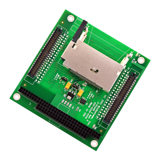
Summary of Contents for WinSystems PCM-CFLASH-2
- Page 1 (217) 352-9330 | Click HERE Find the WinSystems PCM-CFLASH2-40-0 at our website:...
- Page 2 OPERATIONS MANUAL PCM-CFLASH-2 NOTE: This manual has been designed and created for use as part of the WinSystems’ Technical Manuals CD and/or the WinSystems’ web site. If this manual or any portion of the manual is downloaded, copied or emailed, the links to additional information (i.e. software, cable drawings) will be inoperable.
- Page 3 REVISION HISTORY P/N 403-0029-000 ECO Number Date Code Rev Level ORIGINATED 011012 04-34 040806 06-18 060314 07-143 080108...
-
Page 4: Table Of Contents
General Information Features Functional Capability Master/Slave Mode Selection Auxiliary Power Input IDE Interface Alternate IDE Interface PC/104 Bus Interface CFLASH Device 3.3V/5V Mode Selection PCM-CFLASH-2 Parts Placement Guide PCM-CFLASH-2 Parts List Jumper Reference PCM-CFLASH-2 Schematic Diagram Specifications WARRANTY REPAIR INFORMATION... - Page 5 This page is left intentionally blank.
- Page 6 Input 1 2 3 4 o o o o NOTE: The reference line to each component part has been drawn to Pin 1, where applicable. Pin 1 is also highlighted with a red square, where applicable. 080108 OPERATIONS MANUAL PCM-CFLASH-2...
-
Page 7: Introduction
Introduction This manual is intended to provide the necessary information regarding configuration and usage of the PCM-CFLASH-2 board. WinSystems maintains a Technical Support Group to help answer questions regarding usage, or programming of the board. For answers to questions not adequately addressed in this manual, contact Technical Support at (817) 274-7553 between 8 a.m. -
Page 8: Functional Capability
1 2 3 4 o o o o The PCM-CFLASH-2 can be used in any of four modes. 1. Stand-alone - no other IDE device. 2. As a master to a slave PCM-CFLASH-2. 3. As a secondary drive to another PCM-CFLASH-2. -
Page 9: Auxiliary Power Input
Auxiliary Power Input Visual When the PCM-CFLASH-2 is not used on a PC/104 stack, power must be supplied via Index the connector at J6. The pin definitions for J6 are shown here: IDE Interface Visual Index The PCM-CFLASH-2 default IDE interface is made via the connectors at J2 and J9. An alternate IDE interface is available at J1 and J8, wtih 44-pin connectors that supply voltage through the extra pins. -
Page 10: Alternate Ide Interface
29 o o 30 INTRQ 31 o o 32 IOCS16* 33 o o 34 35 o o 36 HDCS0 37 o o 38 HDCS1 39 o o 40 41 o o 42 43 o o 44 080108 OPERATIONS MANUAL PCM-CFLASH-2... -
Page 11: Pc/104 Bus Interface
NOTES: 1. Rows C and D are not required on 8-bit modules. 2. B10 and C19 are key locations. WinSystems uses key pins as connections to GND. 3. Signal timing and function are as specified in ISA specification. 4. Signal source/sink current differ from ISA values. -
Page 12: Cflash Device 3.3V/5V Mode Selection
3.3V (J10 = 2-3). Unless the CompactFlash manufacturer recommends otherwise, we suggest that you operate this device using 3.3V. 1 2 3 1 2 3 o o o o o o 3.3 Volt Mode 5 Volt Mode (Default) 080108 OPERATIONS MANUAL PCM-CFLASH-2... -
Page 13: Pcm-Cflash-2 Parts Placement Guide
PCM-CFLASH-2 Parts Placement Guide 080108 OPERATIONS MANUAL PCM-CFLASH-2... -
Page 14: Pcm-Cflash-2 Parts List
PCM-CFLASH-2 Parts List ASSM ITEM FROM: PCM-CFLASH2-40-0 ASSM ITEM THRU: PCM-CFLASH2-40-0 PARENT LOC FROM: <FIRST> DEFAULT COMPONENT LOCATION: ARLIN PARENT LOC THRU: <LAST> =================================================================================================================================== ITEM LVL ITEM KEY ITEM DESCRIPTION BOM COMMENT TYPE REQUIRED =================================================================================================================================== PCM-CFLASH2-40-0 PC/104, 16-BIT, 0MB, TYPE 2 COMPACT... -
Page 15: Jumper Reference
Input 1 2 3 4 o o o o NOTE: The reference line to each component part has been drawn to Pin 1, where applicable. Pin 1 is also highlighted with a red square, where applicable. 080108 OPERATIONS MANUAL PCM-CFLASH-2... -
Page 16: Pcm-Cflash-2 Schematic Diagram
PCM-CFLASH-2 Schematic Diagram 080108 OPERATIONS MANUAL PCM-CFLASH-2... -
Page 17: Specifications
P C/104-Bus: COMM CON 50711C-104G Environmental Operating Temperature :-40°C to +85°C using industrial drives Non-condensing relative Humidity :8% to 95% Vibration :15 G Peak to Peak Shock :2000 G Max. (All parameters depend on media used.) 080108 OPERATIONS MANUAL PCM-CFLASH-2... -
Page 18: Warranty Repair Information
Notwithstanding anything herein to the contrary, this warranty granted by WinSystems to the Customer shall be for the sole benefit of the Customer, and may not be assigned, transferred or conveyed to any third party. The sole obligation of WinSystems for...
Need help?
Do you have a question about the PCM-CFLASH-2 and is the answer not in the manual?
Questions and answers