
Subscribe to Our Youtube Channel
Related Manuals for LG SH2


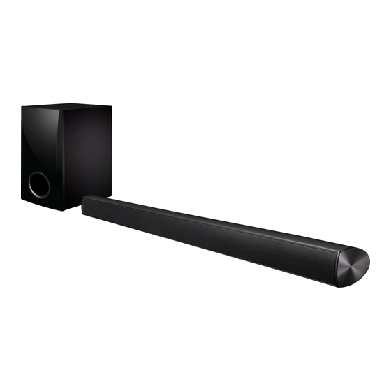
Summary of Contents for LG SH2
- Page 1 Internal Use Only 2.1 ch Sound Bar SERVICE MANUAL MODEL: SH2 (SH2, SPH2B-P) CAUTION BEFORE SERVICING THE UNIT, READ THE “SAFETY PRECAUTIONS” IN THIS MANUAL. P/NO : AFN77457385 MARCH, 2016...
- Page 2 CONTENTS SECTION 1 ..GENERAL SECTION 2 ..CABINET & MAIN CHASSIS SECTION 3 ..ELECTRICAL SECTION 4 ..REPLACEMENT PARTS LIST...
- Page 3 SECTION 1 GENERAL CONTENTS ESD PRECAUTIONS ............................1-3 HIDDEN KEY MODE ............................1-4 FIRMWARE UPDATE ............................1-5 SPECIFICATIONS ............................. 1-6...
-
Page 4: Esd Precautions
ESD PRECAUTIONS Electrostatically Sensitive Devices (ESD) Some semiconductor (solid state) devices can be damaged easily by static electricity. Such components commonly are called Electrostatically Sensitive Devices (ESD). Examples of typical ESD devices are integrated circuits and some field-effect transistors and semiconductor chip components. The following techniques should be used to help reduce the incidence of component damage caused by static electricity. -
Page 5: Hidden Key Mode
HIDDEN KEY MODE ENTRANCE EXIT HIDDEN MODE DISPLAY RESULT SW version will be output by voice through Speaker with below order. You can select each version by Volume +/- key. 1) DSP 2) CHECKSUM Front ‘Vol(-)’ + Remote control 3) Touch IC Version Remote control ‘STANDARD’,... -
Page 6: Firmware Update
FIRMWARE UPDATE 1. To update the Firmware 1) Copy the fi rmware upgrade fi le to a empty USB device. Make sure the USB device is empty before transferring the fi rmware upgrade fi le. 5) Complete the fi rmware update. When the update is successfully completed, the unit goes into the standby mode after the automatic reset. -
Page 7: Specifications
SPECIFICATIONS • GENERAL Power requirements 120 V ~ 60 Hz Power consumption 25 W Networked standby : 0.5 W (If all network ports are activated.) Dimensions (W x H x D) Approx. 880 mm x 62 mm x 90 mm (34.6 inch x 2.4 inch x 3.5 inch) Net Weight Approx. - Page 8 SECTION 2 CABINET & MAIN CHASSIS CONTENTS EXPLODED VIEWS ............................2-3 1. MAIN UNIT SECTION ..........................2-3 2. SUBWOOFER SECTION .......................... 2-7 3. PACKING ACCESSORY SECTION ......................2-8...
-
Page 10: Exploded Views
EXPLODED VIEWS 1. MAIN UNIT SECTION NOTES) THE EXCLAMATION POINT WITHIN AN EQUILATERAL TRIANGLE IS INTENDED TO ALERT THE SERVICE PERSONNEL TO THE PRESENCE OF IMPORTANT SAFETY INFORMATION IN SERVICE LITERATURE. CABLE5 CABLE3 SMPS CABLE4 MAIN TOUCH KEY CABLE2 JACK CABLE6 CABLE1... -
Page 12: Subwoofer Section
2. SUBWOOFER SECTION A900... -
Page 13: Packing Accessory Section
3. PACKING ACCESSORY SECTION Owner’s manual 835 Wall bracket Optical cable 836 Screws Remote control 804 Bag Packing, Main 802 Box... -
Page 14: Table Of Contents
SECTION 3 ELECTRICAL CONTENTS ONE POINT REPAIR GUIDE ..........................3-2 1. NO POWER PROBLEM ......................... 3-2 2. SPEAKER NO SOUND ........................... 3-3 3. PORTABLE FUNCTION DOESN’T WORK (OPTIONAL PART) ............3-4 4. BT FUNCTION DOESN’T WORK ......................3-5 5. OPTICAL FUNCTION DOESN’T WORK ....................3-6 6. -
Page 15: One Point Repair Guide
ONE POINT REPAIR GUIDE 1. NO POWER PROBLEM No power problem occurs when you power on. (No LED Sens.) 1-1. DSP (Micom) IC101 1-1-1. Solution Replace IC101, IC105, X101 on MAIN board. 1-1-2. How to troubleshoot (Countermeasure) 1) Please check Vcc voltage. (pin A4, A10, D4, D14, P4, P14, U5, U6, U9 of IC101 3.3 V) If 3.3 V voltage doesn’t come out, Replace IC602. -
Page 16: Speaker No Sound
ONE POINT REPAIR GUIDE 2. SPEAKER NO SOUND No Sound when you TURN ON the unit. 2-1. Digital AMP (IC701, IC702) 2-1-1. Solution Replace IC701, IC702 on MAIN board. 2-1-2. How to troubleshoot (Countermeasure) 1) Please check 3.3 V of IC701, IC702 pin13. If 3.3 V voltage doesn’t come out, Replace IC602. -
Page 17: Portable Function Doesn't Work (Optional Part)
IC921 EUROPE < Schematic point > CN104 CN103 RC201 Debug IC921 IC921 Debug Monitor R24FV1A PN551 P/N : 6870S-0036A DOWNLOAD JIG SH2 PV [MAIN] R936 R938 X201 R218 R217 R935 C924 24.576MHz(SX-1) R223 R221 2015. 11. 27 C922 C927 R665... -
Page 18: Bt Function Doesn't Work
PGPC03 PGPC04 PGPC05 R137 PGPC06 PN261 PN261 VDD33IO C107 R138 VSS33IO R139 < Schematic point > P/N : 6870S-0036A DOWNLOAD JIG SH2 PV [MAIN] R936 R938 X201 R218 R217 R935 C924 24.576MHz(SX-1) R223 R221 2015. 11. 27 C922 C927 R665... -
Page 19: Optical Function Doesn't Work
R109 R111 < Schematic point > CN104 CN103 RC201 Debug Debug Monitor R24FV1A PN551 P/N : 6870S-0036A X201 X201 DOWNLOAD JIG SH2 PV [MAIN] R936 R938 X201 R218 R217 R935 C924 24.576MHz(SX-1) 2015. 11. 27 R223 R221 C922 C927 R665... -
Page 20: Protection
ONE POINT REPAIR GUIDE 6. PROTECTION 6-1. Protection-1 6-1-1. Solution Replace IC701, IC702 (AMP IC) on MAIN board. 6-1-2. How to troubleshoot (Countermeasure) 1) After MAIN SET power off, check Red LED blink at intervals of 1 sec. 2) Turn MAIN SET power on again. 3) Check PVDD voltage (21 V) of PN601 pin1, 2. - Page 21 3) Check voltage 3.3 V of AMP_FAULT signal (pin14 of IC701, IC702). 4) If pin14 of IC701, IC702 is low (0 V), Replace IC701, IC702 (AMP IC) on MAIN bottom board. 6-2-3. Service hint (Any picture / Remark) P/N : 6870S 0036A DOWNLOAD JIG SH2 PV [MAIN] R936 R938 X201 R218...
-
Page 22: Electrical Troubleshooting Guide
ELECTRICAL TROUBLESHOOTING GUIDE 1. SMPS PART (POWER ON) Start (AC In) Voltage between pin1 & 2 of the CN21 Check the F1, U1, R24, R25, R26. is whether 21 V? Clear Check the RS1, R9, C8. Repair the components described above. YES (Clear) Please check the Main board. -
Page 23: System Part
ELECTRICAL TROUBLESHOOTING GUIDE 2. SYSTEM PART Power On LED on Function OK? IC601 M3.3 VA OK? Check IC604 and SMPS. IC603 1.2 VA OK? Check IC604 and SMPS. MAIN Board X101 24 MHz OK? Replace X101. IC501 function key in Check IC501, IC101. -
Page 24: Audio Output
ELECTRICAL TROUBLESHOOTING GUIDE 3. NO AUDIO OUTPUT Optical function IC201 pin6 Check PN508, JK551 or Replace. OPT_IN signal OK? IC101 F1, F2, G1, G2 Check IC201 or Replace. I2S signal OK? IC101 D1, D2, E1, E4 Check IC101 or Replace. I2S signal OK? Check IC701, IC702 output stage and speaker terminal. -
Page 25: Waveforms Of Major Check Point
WAVEFORMS OF MAJOR CHECK POINT 1. SYSTEM PART-1 (X-TAL) FIG 1-1. DIR (IC201) - CS8422 FIG 1-2. DSP (IC101) - MLC3730SD PGPB08 PGPD10 PAD(3) VDD12INT PGPD09 PSDDQM(0) VSS12INT VDD12CORE PGPB09 PGPC12 VSS12CORE PGPB10 PGPC13 PSDDQM(1) PGPB11 PGPD08 PGPC14 PSDCKE PGPD07 PGPB12 PGPD06 PGPC15... -
Page 26: System Part-2 (I2S Signal)
2. SYSTEM PART-2 (I2S SIGNAL) DATA MCLK LRCK FIG 2-1. AMP (IC701, IC702) - TAS5733 FIG 2-2. AMP (IC701, IC702) - TAS5733 C732 R719 C731 C712 C734 C711 2P 2.5mm R720 C733 PN701 NO VIA, CLOSE TO IC L701:1 C701 C702 R701 IC701... -
Page 27: System Part-3 (I2C Signal)
3. SYSTEM PART-3 (I2C SIGNAL) DIR_SCL TOUCH_SCL DIR_SDA TOUCH_SDA FIG 3-1. DIR (IC201) - CS8422 FIG 3-2. TOUCH (IC501) - TC354K L501 R203 IC501 R211 R212 R213 R214 R215 R216 R217 R221 R222 FB221 3-14... -
Page 28: Wiring Diagram
WIRING DIAGRAM SPK(WOOFER) OPTICAL PORTABLE 90 mm, 1P, #24, JACK JACK JACK JACK(SVC) LED PCB 712AX-BS-2 PN502 8P 60 mm 1.0 mm FFC JACK PCB PN502 TOUCH KEY PCB 2P 140 mm To CHASSIS MAIN 2.5 mm 10P 110 mm 1.0 mm FFC BT MODULE MAIN PCB... -
Page 29: Block Diagrams
BLOCK DIAGRAMS 1. SYSTEM BLOCK DIAGRAM 3-17 3-18... -
Page 30: Power Block Diagram
2. POWER BLOCK DIAGRAM 3-19 3-20... -
Page 31: Circuit Diagrams
DESIGN BE MODIFIED OR ALTERED WITHOUT DIFFER FROM THE ACTUAL CIRCUIT USED. THIS 2. Voltages are DC-measured with a digital voltmeter PERMISSION FROM THE LG CORPORATION. ALL WAY, IMPLEMENTATION OF THE LATEST SAFETY during Play mode. COMPONENTS SHOULD BE REPLACED ONLY WITH... -
Page 32: Main - Amp & Power Circuit Diagram
2. MAIN - AMP & POWER CIRCUIT DIAGRAM R911 AMP CLIP DETECT CIRCUIT C926 Q755 100nF R775 IC921 R771 C921 R767 R939 Q756 C922 Q753 R940 R766 Slave Mode I2S, 24Bit D753 Q754 C929 R764 R770 100nF ADD PV 16 POINT C732 EUROPE R719... -
Page 33: Main - Dsp Circuit Diagram
3. MAIN - DSP CIRCUIT DIAGRAM RC201 IC105 R19E R19H R19N R19P R203 R19Q C231 R136 R211 R235 R212 R130 R917 R234 R213 R233 FB101 R214 R232 R215 R231 R216 R217 C101 C102 C133 VDD33IO RA102 VDD33IO VSS33IO R221 VSS33IS PD(14) R222 RA103... -
Page 34: Jack/ Led/ Touch Key Circuit Diagram
LUG501 LD501 PORTABLE OPTICAL BLUTOOTH LG TV STBY (MUTE) OPTION : PORTABLE FUNCTION MLC3730,A2 : HIGH OPTICAL / BT / LG TV / PORTABLE MLC3730,A2 : LOW : WAVEFORM NUMBER OPTICAL / BT / LG TV / MUTE 3-27 3-28... -
Page 35: Circuit Voltage Chart
CIRCUIT VOLTAGE CHART 1. ICs 3. CAPACITORS Location No Description Source Spec Range[V] Measure [V] Location No Value (uF) Voltage_Spec Measure Margin M3.3VA 3.135~ 3.465 3.32 C3, C4 330 pF OSC_3.3VA 3.135~ 3.465 3.32 IC101 MLC3730D 1.2VA 1.08 ~1.32 1.22 C6 (Peak to Peak) 2200 pF USB_1.2V... -
Page 36: Connectors
4. CONNECTORS Connector No. SOURCE SPEC(V) Value(V) SMPS Board PVDD 19.5 ~ 21.5 20.5 PVDD 19.5 ~ 21.5 20.5 PN601 CN21 (SMPS) DGND DGND MAIN Board VCC55 4.65 ~ 5.35 5.14 JK553 DGND 3V3_MICOM 3.14~3.47 3.32 DGND TOUCH_IRQ 2.3~3.47 3.32 PN110 TOUCH_SDA 2.3~3.47... -
Page 37: Printed Circuit Board Diagrams
PRINTED CIRCUIT BOARD DIAGRAMS 1. SMPS P. C. BOARD DIAGRAM (TOP VIEW) NOTE) Warning Parts that are critical with respect to risk of fire or electrical shock. (BOTTOM VIEW) 3-33 3-34... -
Page 38: Main P. C. Board Diagram
2. MAIN P. C. BOARD DIAGRAM (TOP VIEW) CN104 CN103 RC201 Debug Debug Monitor PN551 R24FV1A P/N : 6870S-0036A DOWNLOAD JIG SH2 PV [MAIN] R936 R938 X201 R218 R217 R935 C924 R223 R221 24.576MHz(SX-1) 2015. 11. 27 C922 C927 R665... -
Page 39: Jack P. C. Board Diagram
3. JACK P. C. BOARD DIAGRAM (TOP VIEW) (BOTTOM VIEW) SH2 PV [JACK] 2015. 11. 26 Rev 2.0 PN505 P/N : 6870S-0037A VCC55 POT_L AGND Assy No POT_R CHECK AGND DGND OPT_OUT 3V3_MICOM 0037A 0037B L551 LUG501 PN508 FB501 C551...
Need help?
Do you have a question about the SH2 and is the answer not in the manual?
Questions and answers