Advertisement
Quick Links
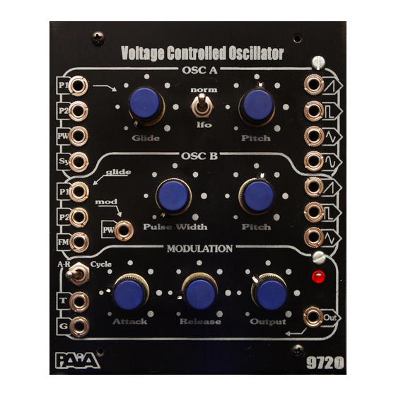
Dual VCO w/Modulator
010321
The 9720 Dual VCO w/Modulator features two independent VCOs,
each with a chromatic range of 10 octaves from 16Hz to 16kHz at a
+/- 1cent pitch error. Total range of each oscillator is from 1 cycle/
minute (0.017 Hz) to 100 kHz so either can be used as wide range
audio source or super slow multi-waveform LFO. Temperature
stability is equally extraordinary due to a novel exponential converter
that provides more accurate temp tracking than conventional designs
without the use of temperature compensating resistors.
Oscillator A has 5V p-p outputs for Ramp, Pulse (w/Width modula-
tion), Triangle and Sin waveforms. The built-in Glide Processor
provides slew rates from milliseconds to several seconds and a
convenient toggle switch transposes down from normal audio outputs
to LFO mode. The Pitch knob sets initial pitch over a 3 octave range.
The Sync input provides for "Soft Synchronization" to an external
Oscillator B is very similar to Osc A but subtle differences optimize
the flexibility of the pair. There are outputs for Ramp, Triangle and
Pulse waveforms. A panel control for initial Pulse Width works in
conjunction with the PW CV input that is normalized to the Modulator
output. An auxiliary 1V/kHz Frequency Modulation input allows for
complex FM timbres from just a single module.
The Modulator is an Attack/Release Envelope Generator that has a
separate Trigger input for A/R envelopes and Gate input for A/R with
Sustain (ASR). Attack time is adjustable from 0.5ms to 2 seconds,
Release time from 1ms to 4 seconds. The Cycle switch allows self-
triggering for an LFO with independently adjustable rise and fall
times and a range from a cycle every few seconds to over 100Hz.
The Gate and Trigger inputs also work when in Cycle mode - a Gate
input turns the oscillator off and on and Trigger inputs syncs the
oscillator to an external source. The front panel LED brightens and
(c) 2000 PAiA Electronics, Inc.
Model 9720
Assembly and Using Manual
dims to indicate Modulator output.
9720 VCO
audio source.
1
Advertisement

Related Manuals for Paia 9720


Summary of Contents for Paia 9720
- Page 1 Model 9720 Assembly and Using Manual The 9720 Dual VCO w/Modulator features two independent VCOs, each with a chromatic range of 10 octaves from 16Hz to 16kHz at a +/- 1cent pitch error. Total range of each oscillator is from 1 cycle/ minute (0.017 Hz) to 100 kHz so either can be used as wide range...
- Page 2 Supplement in the center of this manual. These pages may be removed for easy reference during assembly. THE CIRCUIT BOARD The 9720 VCO is built on a double-sided circuit board. No special preparation or cleaning is necessary before assembly. The "top" of the board is the side that is printed with component designations and parts are mounted from this side.
- Page 3 Scott Lee Use care when mounting all components. Never force Mike Murphy a component into place. Johnny Klonaris David Hillel Wilson and me - John Simonton 010321 9720 VCO...
- Page 4 Clip each lead flush with the solder joint and save a few of the clippings for use in later steps. The 9720 VCO uses 1% film resistors in precision circuitry and 5% carbon film resistors in non-critical locations. Not all resistors are mounted on the circuit board, some will be "left over"...
- Page 5 ( ) R41 390k orange-white-yellow ( ) R28 orange-white-orange ( ) R55 orange-white-orange ( ) R30 470k yellow-violet-yellow listed below: 47k yellow-violet-orange ( ) R39 ( ) R69 ( ) R92 ( ) R105 ( ) R2 green-blue-black 010321 9720 VCO...
- Page 6 ( ) R16 ( ) R40 ( ) R42 Disk and Polystyrene Capacitors Many of the capacitors used in the 9720 are nonpolarized 1% Resistors have Ceramic Disk and Polystyrene types. For each of these, 5 color bands either lead can go in either of the holes in the circuit board.
-
Page 7: Electrolytic Capacitors
VALUE ( ) C12 1uF / 15V. ( ) C22 1uF / 15V. ( ) C1 470uF / 25V. ( ) C2 470uF / 25V. ( ) C4 4.7uF / 15V ( ) C6 4.7uF / 15V 010321 9720 VCO... - Page 8 The straight line of the pc ( ) Q4 not matched graphic symbol corresponds to the flat face of the listed below: 2N3904 NPN Si Transistors not matched transistor case. ( ) Q5 ( ) Q6 ( ) Q7 ( ) Q10 9720 VCO 010321...
-
Page 9: Integrated Circuits
Make sure that the part is seated firmly against the circuit board by pressing it down while re- melting the solder joint at first one corner, then the other. Finally, solder the remaining connections. 010321 9720 VCO... -
Page 10: Voltage Regulators
Trim the longer lead off flush with the solder joint - the shorter lead may need no trimming. DESIGNATION TYPE Use 1/2" length of the small diameter sleeving ( ) LED1 Red LED as a spacer and insulator on the LED. 9720 VCO 010321... -
Page 11: "Flying" Wires
( ) "AF" 8" This completes assembly of the 9720 circuit board. Admire your work for a few minutes then take a break. When you come back, admire your work again but this time be critical. It would be a good time to double check the orientation of polarized parts and that the right resistors and capacitors are in the right places. - Page 12 Orient the switches as shown in fig 3 and fully be supplied even though only SPST tighten the nut to secure it. The switch is are required. symmetrical so whichever soldering lug is on the left or up is #1. 9720 VCO 010321...
- Page 13 R205-3 (ns) ( ) 3-1/4" S2-1 (s1) R204-1 (ns) ( ) 2" R204-1 (ns) R202-1 (ns) ( ) 3/4" R206-1 (ns) J10-S (ns) ( ) 3/4" J7-X (ns) S1-2 (ns) Many point-to-point panel connections are made using the 010321 9720 VCO...
- Page 14 Cut a 3/8" long piece of large tubing from the length supplied connection and slip it over the wire before making the connection. When the solder joint has cooled, slide the tubing down over the lug (see fig 4). FROM FROM 9720 VCO 010321...
- Page 15 ( ) "J" R205-1 (s1) ( ) "O" J6-T (s1) ( ) "Y" R205-3 (s2) ( ) "AF" J9-T (s2) ( ) "T" J10-T (s1) ( ) "X" J5-X (s1) ( ) "Z" J1-T (s2) POWER CABLE AND CONNECTOR 010321 9720 VCO...
- Page 16 97xx Module before soldering in place. Clip off any excess on the solder side of the board. Use the 3 nylon wire ties to group the four wires together by placing 9720 VCO 010321...
- Page 17 1) Set the 9720 knobs and switch as shown and turn on power. First observe the POWER light on the power supply and if it doesn't come on stop and find out why.
- Page 18 IC4, Q2, Q3 and associated components. If OscB is not functioning properly IC5, Q8, Q9 and components associated with them should be examined. These ramp outputs must be working before any of the others will work properly. 9720 VCO 010321...
- Page 19 Oscilloscope, Frequency Counter or digital voltmeter is available. If you have this kind of equipment it may be used and there are some tips and pointers at http://paia.com/ 9720test.htm. But the results produced using this equipment will be no more accurate the equipment-free procedure that follows.
- Page 20 ) of OscA and OscB and arrange for both to be heard at the same time at approximately equal amplitudes. If a PAiA 9710 Triple VCA is available it's L and R inputs can be used to mix the two to a single output.
-
Page 21: The Panel Controls
3 octaves. With no external CV inputs each oscillator produces a pitch of approximately C (C below middle C) at "max" fully ClockWise rotation and C at "min" fully CounterClockWise rotation. OscA Pitch CV Input 1. This 1V/oct scaled 010321 9720 VCO... - Page 22 Triangle Output- Odd and even harmonics Odd harmonics only Pulse Output Sine Output Harmonics depend on DF About 5% harmonic distortion. OscA Glide. Sets how fast oscillators respond to Pitch CV changes. At "min" fully CCW the 9720 VCO 010321...
- Page 23 THE BLOCK DIAGRAM Fig 6 in the illustrations supplement shows Calibrate Init Pitch for the organization and normalization of the panel controls, inputs R52 to calibrate to .8V and outputs. LFO Sync / Gate OscA LFO function vari Design Analysis 010321 9720 VCO AR Cycle A= 1ms to 8s...
- Page 24 Oscillators - The two VCOs in the 9720 have essentially identical core elements. Taking OscA as typical, IC7:A, IC6:D and Q10 are the active elements in a relaxation oscillator topology. C11 is the timing capacitor which is charged by a current source to be described shortly. As C11 charges a linear voltage ramp is produced across the capacitor.
- Page 25 18mV/oct needed at Q2's b-e junction. The 9720 expos take a slightly different approach here and instead use the two stages of an LM13700 type Operational Transconductance Amplifier (IC4) to perform this summing and scaling function.
- Page 26 (S1) is closed, this negative transition is coupled by R67 and C22 to the base of Q6 and unconditionally turns this transistor off. Q6's now high collector voltage turns Q5, and consequently Q4, on - starting the Attack cycle again. 9720 VCO 010321...
- Page 27 010321 9720 VCO...
- Page 28 9720 Parts List qnty description designation orange-white-orange *R208,R28,R55 Semiconductors 470k yellow-violet-yellow R30 1N4148 or 1N914 Si diodes D1-D18 yellow-violet-orange R39,R69,R92,R105 red LED LED1 green-blue-black 7812 +12V Regulator 5600 green-blue-red R64,R82,R36,R37 7912 -12V Regulator green-blue-orange R20,R23,R44,R48, TL084 Quad FET OpAmps IC3,IC7...
Need help?
Do you have a question about the 9720 and is the answer not in the manual?
Questions and answers