Table of Contents
Advertisement
Quick Links
Intel Skylake-U / Kaby Lake-U Core i CPU,
DDR4 2133 MT/s SODIMM, 2 x LAN / 2 x HDMI / USB /
2 x Intel GbE LAN, 2 x PCIe mini card slots, 2 x HDMI, eD P
4 x USB 3.0, 3 x USB 2.0, 2 x COM, Wide Range DC-IN
CAUTION
RISK OF EXPLOSION IF BATTERY IS REPLACED
BY AN INCORRECT TYPE.
DISPOSE OF USED BATTERIES ACCORDING
TO THE INSTRUCTIONS
NO. 2I612CW
Release date: Feb. 18. 2020
2I612CW
COM / PCIe mini card
Intel Skylake-U / Kaby Lake-U Core i CPU,
All-In-One
,
Advertisement
Table of Contents

Subscribe to Our Youtube Channel
Summary of Contents for Tera 2I612CW
- Page 1 4 x USB 3.0, 3 x USB 2.0, 2 x COM, Wide Range DC-IN CAUTION RISK OF EXPLOSION IF BATTERY IS REPLACED BY AN INCORRECT TYPE. DISPOSE OF USED BATTERIES ACCORDING TO THE INSTRUCTIONS NO. 2I612CW Release date: Feb. 18. 2020...
-
Page 2: Table Of Contents
CHAPTER 2 HARDWARE INSTALLATION ..............2-1 UNPACKING PRECAUTION ..................2-2 UNPACKING CHECKUP ....................2-3 DIMENSION-2I612CW ....................2-4 LAYOUT-2I612CW-CONNECTOR AND JUMPER TOP ..........2-4-1 LAYOUT-2I612CW-CONNECTOR AND JUMPER BOT ..........2-5 LAYOUT-2I612CW-FUNCTION MAP TOP ..............2-5-1 LAYOUT-2I612CW-FUNCTION MAP BOT ............... 2-6 DIAGRAM-2I612CW TOP .................... - Page 3 3-10 I BUS INTERFACE ....................3-11 DC POWER INPUT ....................3-12 CPO1: +12 / +5V DC VOLTAGE OUTPUT 1x4 PIN (2.0MM) WAFER (BLACK) ..3-13 SATA INTERFACE ..................... 3-14 DISPLAY INTERFACE ....................3-15 EDP1: EDP INTERFACE 2x10 PIN (1.25MM) WAFER ..........3-16 MPCE1 PCI EXPRESS MINI CARD ................
- Page 4 5-7 HOW TO UPDATE INSYDE BIOS ................
- Page 5 Copyright This manual is copyrighted and all rights are reserved. It does not allow any non authorization in copied, photocopied, translated or reproduced to any electronic or machine readable form in whole or in part without prior written consent from the manufacturer. In general, the manufacturer will not be liable for any direct, indirect, special, incidental or consequential damages arising from the use of inability to use the product or documentation, even if advised of the possibility of such damages.
-
Page 6: Warning
Warning ! Battery Batteries on board are consumables. The life time of them are not guaranteed. 2. Fanless solution with HDD The specifi cation & limitation of HDD should be considered carefully when the fanless solution is implemented. We will not give further notifi cation in case of changes of product information and manual. -
Page 7: Hardware Notice Guide
Hardware Notice Guide 1. Before linking power supply with the motherboard, please attach DC-in adapter to the motherboard fi rst. Then plug the adapter power to AC outlet. Always shut down the computer normally before you move the system unit or remove the power supply from the motherboard. - Page 8 Photo 1 Insert Unplug...
-
Page 9: Chapter 1 General Information
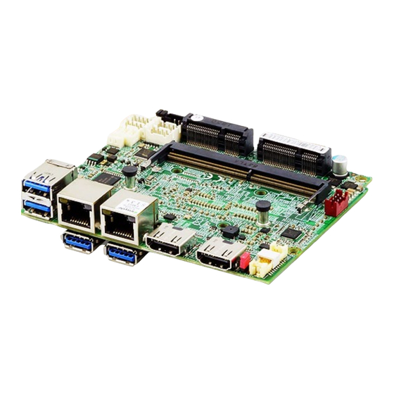
Chapter-1 General Information The 2I612CW is a 2.5" (110 x 92 mm) motherboard powered with Intel® Skylake-U processor & offered the ideal platform for high performance applications. The ultra compact (110 x 92 mm) motherboard with wide range 9~36V DC power input & embeds multiple Intel GbE LAN, USBs, COM Ports and VGA display interface that off... -
Page 10: Major Feature
1-1 Major Feature Intel® Celeron 3955U Processor 2.0GHz, (Dual core), Intel® Core i5-6200U Processor 2.3GHz / 2.8GHz (Dual core), Intel® Core i7-6600U Processor 2.6GHz / 3.4GHz (Dual core) Intel 9th generation (Gen 9) LP graphics and media encode / decode engine, Intel® Celeron 3955U 300MHz / 900MHz, Intel®... -
Page 11: Specification
1-2 Specifi cation SOC: Intel® Celeron 3955U Processor 2.0GHz, (Dual core), Intel® Core i5-6200U Processor 2.3GHz / 2.8GHz (Dual core), Intel® Core i7-6600U Processor 2.6GHz / 3.4GHz (Dual core) Memory: DDR4 SODIMM slot x 1, up to 16GB Graphics: Intel 9th generation (Gen 9) LP graphics and media encode / decode engine, Intel®... -
Page 12: Installing The So-Dimm
1-3 Installing the SO-DIMM 1. Align the SO-DIMM with the connector at a 45 degree angle. 2. Press the SO-DIMM into the connector until you hear a click. - Page 13 Notices: 1.The connectors are designed to ensure the correct insertion. If you feel resistance, check t h e connectors & golden fi nger direction, and realign the card. 2. Make sure the retaining clips (on two sides of the slot) lock onto the notches of the card fi...
-
Page 14: Removing The So-Dimm
1-3-1-1 Removing the SO-DIMM 1. Release the SO-DIMM by pulling outward the two retaining clips and the SO-DIMM pops up slightly. 2. Lift the SO-DIMM out of its connector carefully. -
Page 15: Installing The Mini Pci-E Card (Full Size)
1-4 Installing the Mini PCI-e Card (Full Size) 1. Unscrew the screw on the board 2. Plug in the Mini Card in a 45 angle 3. Gently push down the Mini Card and screw the screw back. -
Page 16: Packing List
Quantity 60W Power 6G5212-0623-0100 L Type,2.5Ø,FSP060-DHAN3,FSP Adapter,12V/5A 6G6003-7350-0100 Power Cable LF, 2.0 2*4/DC JK,L=9cm 7G1901-2042001-0 MB-2I612CW-EC0-001 LF,2I612CW-EC0,Rev.:001 Optional accessories (items in addition to motherboard) are not included in the standard packing. Please contact your dealer to purchase the optional accessories. -
Page 17: Chapter 2 Hardware Installation
Chapter-2 Hardware Installation 2-1 Unpacking Precaution This chapter provides the information how to install the hardware of 2I612CW. Please follow section 1-5, 2-1 and 2-2 to check the delivery package and unpack carefully. Please follow the jumper setting procedure. NOTE! 1. -
Page 18: Unpacking Checkup
2-2 Unpacking checkup First of all, please follow all necessary steps of section 2-1 to protect 2I612CW from electricity discharge. With reference to section 1-5 please check the delivery package again with following steps: 1. Unpack the 2I612CW board and keep all packing material, manual and driver disc etc, do not dispose ! 2. -
Page 19: Dimension-2I612Cw
2-3 Dimension-2I612CW... -
Page 20: Layout-2I612Cw-Connector And Jumper Top
2-4 Layout-2I612CW-Connector and Jumper CIO1 CFP1 CBT1 CU34 JSB1 JSB2 CPO1 MPCE2 SODIM1 HDMI2 MPCE1 HDMI1 JVL1 EDP1 CPI1... -
Page 21: Layout-2I612Cw-Connector And Jumper Bot
2-4-1 Layout-2I612CW-Connector and Jumper Bottom SATA1... -
Page 22: Layout-2I612Cw-Function Map Top
2-5 Layout-2I612CW-Function MAP USB2.0 4DI/4DO SMBus Front Panel Battery Wafer USB2.0/3.0x2 CMOS Data Clear Power In Always ON COM1 +12V/+5V Output COM2 LAN2 PCIe/USB2.0 /USB3.0 LAN1 DDR4 SODIMM HDMI2 Display port2 PCIe/USB2.0 /mSATA Display port1 HDMI1 eDP Panel Power Select... -
Page 23: Layout-2I612Cw-Function Map Bot
2-5-1 Layout-2I612CW-Function MAP SATA USB2.0/3.0 USB2.0/3.0... -
Page 24: Diagram-2I612Cw Top
2-6 Diagram- 2I612CW CIO1 CFP1 CBT1 CU34 JSB1 JSB2 CPO1 MPCE2 SODIM1 HDMI2 MPCE1 HDMI1 JVL1 CPI1 EDP1... -
Page 25: Diagram-2I612Cw Bot
2-6-1 Diagram- 2I612CW SATA1... -
Page 26: Function Map-2I612Cw
2-6-2 Function MAP- 2I612CW SMBus USB2.0 4DI/4DO Front Panel Battery Wafer CMOS Data Clear Power In Always ON +12V/+5V Output COM2 COM1 PCIe/USB2.0/USB3.0 PCIe/USB2.0/mSATA eDP Panel Power Select DC-IN +9V~+36V USB 3.0 HDMI USB 3.0... -
Page 27: List Of Jumpers
2-7 List of Jumpers JSB1: CMOS DATA Clear JSB2: Power in always ON function JVL1: eDP panel power select 2-8 Jumper Setting Description A jumper is ON as a closed circuit with a plastic cap covering two pins. A jumper is OFF as an open circuit without the plastic cap. -
Page 28: Jsb1: Cmos Data Clear
2-9 JSB1: CMOS DATA Clear A battery must be used to retain the motherboard confi guration in CMOS RAM. Close Pin1 and pin 2 of JSB1 to store the CMOS data. To clear the CMOS, follow the procedures below: 1. Turn off the system and unplug the AC power 2. -
Page 29: Jsb2: Power In Always On Function
2-10 JSB2: Power in always ON function JSB2 DESCRIPTION *1-2 Disabled Enable NOTE: Power always on function default is disabled. JSB2 *Disabled Enable 2-11 JVL1: eDP panel power select JVL1 DESCRIPTION *2-3 +3.3V NOTE: Attention! Check Device Power in spec. JVL1 *+3.3V... -
Page 30: Chapter 3 Connection
Chapter-3 Connection This chapter provides all necessary information of the peripheral's connections, switches and indicators. Always power off the board before you install the peripherals. 3-1 List of Connectors CBT1: CMOS Battery in 1x2 pin (1.25mm) wafer CU1: USB 3.0 type A connector CU2: USB 3.0 type A connector CU34:... -
Page 31: Cmos Battery Connector
3-2 CMOS battery connector CBT1: CMOS Battery in 1x2 pin (1.25mm) wafer PIN NO. DESCRIPTION Battery in (GND) Battery in (+3V) NOTE: CBT1 for external connector can extend battery capacity. CBT1 pin1... -
Page 32: Cu1.Cu2.Cu34: Usb 3.0 / 2.0 Type A Connector
3-3 CU1.CU2.CU34: USB 3.0 / 2.0 Type A connector PIN NO. DESCRIPTION PIN NO. DESCRIPTION USB 3.0 TX+ USB 2.0 D- USB 3.0 TX- USB 2.0 D+ USB 3.0 RX+ USB 3.0 RX- CU34 3-4 CU7.CU8.CU9: USB2.0 1x4 pin (1.25mm) wafer PIN NO. -
Page 33: Cl1.Cl2: Rj45 Lan Connector
3-5 CL1.CL2: RJ45 LAN Connector PIN NO. DESCRIPTION PIN NO. DESCRIPTION TD0+ / TX+ TD0- / TX- TD1+ / RX+ TD2+ / NC TD2- / NC TD1-/ RX- TD3+ / NC TD3- / NC RJ45 LAN Connector---LED defi ne Giga / 100 / 10MB Connector Speed 10 Mbps 100 Mbps... -
Page 34: Com Interface
3-7 COM interface CC1.CC2: COM1 / COM2 2x5 pin (2.0mm) wafer RS232 Mode PIN NO. DESCRIPTION PIN NO. DESCRIPTION Note: 1. COM 1 / 2 Default RS232, RS485 / RS422 by BIOS control. 2. The pin9 RI can be modify to Power to supply device. The power voltage can be set +12V or +5V. -
Page 35: Front Panel Pin Header
3-8 Front Panel Pin Header CFP1: Front Panel 2x5 pin (2.0mm) wafer PIN NO. DESCRIPTION PIN NO. DESCRIPTION Power button pin Power button GND Reset pin Reset GND Power LED Power LED+ HDD LED- HDD LED+ LAN LED- LAN LED+ CFP1 pin1... -
Page 36: Digital Input / Output / Watch Dog Time
3-9 Digital Input / Output / Watch Dog Time CIO1: DIO 0~3 2x5 pin (2.0mm) wafer PIN NO. DESCRIPTION PIN NO. DESCRIPTION DI-0 DO-3 DI-1 DO-2 DI-2 DO-1 DI-3 DO-0 Note: 1. DI pin default pull up 10KΩ to +5V 2. -
Page 37: Io Device: F75111 Under Dos
3-9-1 IO Device: F75111 under DOS The Sample code source you can download from Source fi le: F75111_Dos_Src.rar http://tprd.info/lexwiki/index.php/IO_Device:F75111_under_DOS Binary fi le: F75111_Dos_Bin.rar USERNAME & PASSWORD: sf How to use this Demo Application 1.Boot Ms-Dos Operating System 2.execute "75WDT.EXE" binary fi le 3.Input 1 to Enable WDT timer or input 0 to Disable it. - Page 38 Introduction Enable Watch Dog Timer WriteI2CByte(I2CADDR, CONFIG, 0x03);//Set Watch Dog Timer function WriteI2CByte(I2CADDR, WDT_TIMER, timer);//Set Watch Dog Timer range from 0-255. WriteI2CByte(I2CADDR, WDT_TIMER_CTL, 0x73);//Enable Watch Dog Timer in second and pulse mode Disable Watch Dog Timer WriteI2CByte(I2CADDR, WDT_TIMER_CTL, 0x00); Time Pause for mini seconds void pause(int time) asm mov ah,0h;...
-
Page 39: Io Device: F75111 Cio Utility
3-9-2 IO Device: F75111 CIO Utility The Sample code source you can download from Source fi le: CIO_Utility_Src_v3.0.5_w.zip http://tprd.info/lexwiki/index.php/IO_Device:F75111_CIO_Utility Binary fi le: CIO_Utility_Bin_v3.0.5_x32_w.zip CIO_Utility_Bin_v3.0.5_x64_w.zip F75113 DLL : F75113.dll We do the demo test with a test tool which DIx connect to DOx with Relay. - Page 40 How to use this Demo Application...
- Page 41 Attention Please:You must be install vcredist_x86.exe when first time you run the F75111_DIO.exe DEMO AP,The vcredist_x86.exe include all required DLL fi le. 1. Press the select your test "2i2o","4i4o","4i4o*2","F75111CIO116","F75113CIO116","8i+8o" 2. start test,select single mode or looptest...
- Page 42 F75111 Layout Picture Introduction F75111 Initial Internal F75111 port address (0x9c) defi ne GPIO1X, GPIO2X, GPIO3X to input or output and Enable WDT function pin Set F75111 DI/DO ( sample code as below Get Input value/Set output value ) DO: InterDigitalOutput(BYTE byteValue)) DI: InterDigitalInput() PULSE mode Sample to setting GP33, 32, 31, 30 output 1mS low pulse signal.
- Page 43 Initial internal F75111 void F75111::InitInternalF75111() this->Write_Byte(F75111_INTERNAL_ADDR,GPIO1X_CONTROL_MODE ,0x00); //set GPIO1X to Input function this->Write_Byte(F75111_INTERNAL_ADDR,GPIO3X_CONTROL_MODE ,0x00); //set GPIO3X to Input function this->Write_Byte(F75111_INTERNAL_ADDR,GPIO2X_CONTROL_MODE ,0xFF); //set GPIO2X to Output function this->Write_Byte(F75111_INTERNAL_ADDR,F75111_CONFIGURATION, 0x03); //Enable WDT OUT function Set output value void F75111::InterDigitalOutput(BYTE byteValue) BYTE byteData = 0; byteData = (byteData &...
- Page 44 Get Input value BYTE F75111::InterDigitalInput() BYTE byteGPIO1X = 0; BYTE byteGPIO3X = 0; BYTE byteData = 0; this->Read_Byte(F75111_INTERNAL_ADDR,GPIO1X_INPUT_DATA,&byteGPIO1X) ; // Get value from GPIO1X this->Read_Byte(F75111_INTERNAL_ADDR,GPIO3X_INPUT_DATA,&byteGPIO3X) ; // Get value from GPIO3X byteGPIO1X = byteGPIO1X & 0xF0; // Mask unuseful value byteGPIO3X = byteGPIO3X &...
- Page 45 defi ne F75111 pin in F75111.h //-------------------------------------------------------------------------------------------------------- #defi ne F75111_INTERNAL_ADDR 0x9C // OnBoard F75111 Chipset #defi ne F75111_EXTERNAL_ADDR 0x6E // External F75111 Chipset //-------------------------------------------------------------------------------------------------------- #defi ne F75111_CONFIGURATION 0x03 // Confi gure GPIO13 to WDT2 Function //-------------------------------------------------------------------------------------------------------- #defi ne GPIO1X_CONTROL_MODE 0x10 // Select Output Mode or Input Mode #defi...
- Page 46 Introduction F75113 Base on 75113.Dll API function as below list F75113_API bool _stdcall F75113_Init(); F75113_API BYTE F75113_GetDigital_Low_Input(); //BDI0-BDI7 F75113_API BYTE F75113_GetDigital_High_Input(); //BDI8-BDI15 F75113_API void F75113_SetDigital_Low_Output(BYTE byteValue); //BDO0-BDO7 F75113_API void F75113_SetDigital_High_Output(BYTE byteValue); //BDO8-BDO15 F75113_API void F75113_SetWDT_Enable(BYTE byteTimer); //For the F75113 on board F75113_API void F75113_SetWDT_Disable();...
-
Page 47: Io Device:f75111 Cio Utility Cio116
3-9-3 IO Device:F75111 CIO Utility CIO116 The Sample code source you can download from Source fi le: CIO_Utility_Src_v3.0.3.tar.gz Binary fi le: CIO_Utility_Bin_v3.0.3_x32.tar.gz CIO_Utility_Bin_v3.0.3_x64.tar.gz http://tprd.info/lexwiki/index.php/IO_Device:F75111_CIO_Utility_CIO116 How to use this Demo Application Before executing the program began, Please switch to the highest authority , continued second F75111 ,chmod 777 and root: \ 1. - Page 48 F75111 Layout Picture Introduction Initial Internal F75111 port address (0x9c) defi ne GPIO1X, GPIO2X, GPIO3X to input or output and Enable WDT function pin Set F75111 DI/DO ( sample code as below Get Input value/Set output value ) DO: InterDigitalOutput(BYTE byteValue)) DI: InterDigitalInput() PULSE mode Sample to setting GP33, 32, 31, 30 output 1mS low pulse signal.
- Page 49 Initial internal F75111 void F75111::InitInternalF75111() this->Write_Byte(F75111_INTERNAL_ADDR,GPIO1X_CONTROL_MODE ,0x00); //set GPIO1X to Input function this->Write_Byte(F75111_INTERNAL_ADDR,GPIO3X_CONTROL_MODE ,0x00); //set GPIO3X to Input function this->Write_Byte(F75111_INTERNAL_ADDR,GPIO2X_CONTROL_MODE ,0xFF); //set GPIO2X to Output function this->Write_Byte(F75111_INTERNAL_ADDR,F75111_CONFIGURATION, 0x03); //Enable WDT OUT function Set output value void F75111::InterDigitalOutput(BYTE byteValue) BYTE byteData = 0; byteData = (byteData &...
- Page 50 Get Input value BYTE F75111::InterDigitalInput() BYTE byteGPIO1X = 0; BYTE byteGPIO3X = 0; BYTE byteData = 0; this->Read_Byte(F75111_INTERNAL_ADDR,GPIO1X_INPUT_DATA,&byteGPIO1X) ; // Get value from GPIO1X this->Read_Byte(F75111_INTERNAL_ADDR,GPIO3X_INPUT_DATA,&byteGPIO3X) ; // Get value from GPIO3X byteGPIO1X = byteGPIO1X & 0xF0; // Mask unuseful value byteGPIO3X = byteGPIO3X &...
- Page 51 defi ne F75111 pin in F75111.h //-------------------------------------------------------------------------------------------------------- #defi ne F75111_INTERNAL_ADDR 0x9C // OnBoard F75111 Chipset #defi ne F75111_EXTERNAL_ADDR 0x6E // External F75111 Chipset //-------------------------------------------------------------------------------------------------------- #defi ne F75111_CONFIGURATION 0x03 // Confi gure GPIO13 to WDT2 Function //-------------------------------------------------------------------------------------------------------- #defi ne GPIO1X_CONTROL_MODE 0x10 // Select Output Mode or Input Mode #defi...
-
Page 52: Io Device:f75111 Cio Utility Console Under Linux
3-9-4 IO Device:F75111 CIO Utility Console under linux The Sample code source you can download from Source fi le: CIO_Utility_Console_L_src_v1.3.tar.gz Binary fi le: CIO_Utility_Console_L_bin_v1.3.tar.gz http://tprd.info/lexwiki/index.php/IO_Device:F75111_CIO_Utility_Console_under_linux How to use this Demo Application 1. The program must control I/O device, when you use this you must change user to root, you can use this command "sudo su"... - Page 53 F75111 Layout Picture Introduction Initial Internal F75111 port address (0x9c) defi ne GPIO1X, GPIO2X, GPIO3X to input or output and Enable WDT function pin Set F75111 DI/DO ( sample code as below Get Input value/Set output value ) DO: InterDigitalOutput(BYTE byteValue)) DI: InterDigitalInput() PULSE mode Sample to setting GP33, 32, 31, 30 output 1mS low pulse signal.
- Page 54 Initial internal F75111 void F75111::InitInternalF75111() this->Write_Byte(F75111_INTERNAL_ADDR,GPIO1X_CONTROL_MODE ,0x00); //set GPIO1X to Input function this->Write_Byte(F75111_INTERNAL_ADDR,GPIO3X_CONTROL_MODE ,0x00); //set GPIO3X to Input function this->Write_Byte(F75111_INTERNAL_ADDR,GPIO2X_CONTROL_MODE ,0xFF); //set GPIO2X to Output function this->Write_Byte(F75111_INTERNAL_ADDR,F75111_CONFIGURATION, 0x03); //Enable WDT OUT function Set output value void F75111::InterDigitalOutput(BYTE byteValue) BYTE byteData = 0; byteData = (byteData &...
- Page 55 Get Input value BYTE F75111::InterDigitalInput() BYTE byteGPIO1X = 0; BYTE byteGPIO3X = 0; BYTE byteData = 0; this->Read_Byte(F75111_INTERNAL_ADDR,GPIO1X_INPUT_DATA,&byteGPIO1X) ; // Get value from GPIO1X this->Read_Byte(F75111_INTERNAL_ADDR,GPIO3X_INPUT_DATA,&byteGPIO3X) ; // Get value from GPIO3X byteGPIO1X = byteGPIO1X & 0xF0; // Mask unuseful value byteGPIO3X = byteGPIO3X &...
- Page 56 defi ne F75111 pin in F75111.h //-------------------------------------------------------------------------------------------------------- #defi ne F75111_INTERNAL_ADDR 0x9C // OnBoard F75111 Chipset #defi ne F75111_EXTERNAL_ADDR 0x6E // External F75111 Chipset //-------------------------------------------------------------------------------------------------------- #defi ne F75111_CONFIGURATION 0x03 // Confi gure GPIO13 to WDT2 Function //-------------------------------------------------------------------------------------------------------- #defi ne GPIO1X_CONTROL_MODE 0x10 // Select Output Mode or Input Mode #defi...
-
Page 57: I 2 Bus Interface
3-10 I C Bus Interface CO1: I C Bus 1x4 pin (1.25mm) wafer PIN NO. DESCRIPTION PIN NO. DESCRIPTION +3.3V C Clock C Data pin1 3-11 DC Power Input CPI1: DC Power input 2x4 pin (2.0mm) wafer (RED) PIN NO. DESCRIPTION 1,2,7,8 3,4,5,6 DC-IN... -
Page 58: Cpo1: +12 / +5V Dc Voltage Output 1X4 Pin (2.0Mm) Wafer (Black)
3-12 CPO1: +12V / +5V DC voltage output 1x4 pin (2.0mm) wafer (BLACK) PIN NO. DESCRIPTION PIN NO. DESCRIPTION +12V Note: Very important check DC-in Voltage. CPO1 pin1 3-13 SATA Interface SATA1: SATA port 1x7 pin connector PIN NO. DESCRIPTION PIN NO. -
Page 59: Display Interface
3-14 Display interface HDMI1/ HDMI2: HDMI type A connector PIN NO. DESCRIPTION PIN NO. DESCRIPTION TMDS DATA2+ TMDS DATA2- TMDS DATA1+ TMDS DATA1- TMDS DATA0+ TMDS DATA0- TMDS CLK+ TMDS CLK- DDC CLK DDC DATA H.P. Detect DP1 / DP2: Display port connector (option) PIN NO. -
Page 60: Edp1: Edp Interface 2X10 Pin (1.25Mm) Wafer
3-15 EDP1: eDP interface 2x10 pin (1.25mm) wafer PIN NO. DESCRIPTION PIN NO. DESCRIPTION Lane-0-DATA- +12V Lane-0-DATA+ +12V Lane-1-DATA- Lane-1-DATA+ Backlight Enable PWM dimming I2C Clock +LCD (5V or 3.3V) I2C Data +LCD (5V or 3.3V) eDP Aux+ +LCD (5V or 3.3V) eDP Aux- EDP_HPD Note:... -
Page 61: Mpce1 Pci Express Mini Card
3-16 MPCE1 PCI Express mini card PIN NO. DESCRIPTION PIN NO. DESCRIPTION mSATA / PCIe detect +3.3V +1.5V +3.3V +3.3V USB-DATA+ USB-DATA- PCIe-TX+ / mSATA-TX+ PCIe-TX- / mSATA-TX- +1.5V PCIe-RX+ / mSATA-RX- MPCE2 PCIe-RX- / mSATA-RX+ +3.3V pin52 PERST# Mechanical Key REFCLK+ REFCLK- pin1... -
Page 62: Mpce2 Pci Express Mini Card
3-17 MPCE2 PCI Express mini card PIN NO. DESCRIPTION PIN NO. DESCRIPTION +3.3V +1.5V +3.3V +3.3V USB-DATA+ USB-DATA- PCIe-TX+ / USB3.0TX+ PCIe-TX- / USB3.0TX- +1.5V PCIe-RX+ / USB3.0RX+ PCIe-RX- / USB3.0RX- +3.3V PERST# Mechanical Key REFCLK+ REFCLK- +1.5V +3.3V Note: MPCE2 support USB 2.0, PCIe or USB 3.0 by BIOS control. -
Page 63: Introduction Of Bios
Chapter-4 Introduction of BIOS The BIOS is a program located in the Flash Memory on the motherboard. This program is a bridge between motherboard and operating system. When you start the computer, the BIOS program gains control. The BIOS first operates an auto-diagnostic test called POST (Power on Self Test) for all the necessary hardware, it detects the entire hardware devices and configures the parameters of the hardware synchronization. -
Page 64: Bios Menu Screen & Function Keys
4-2 BIOS Menu Screen & Function Keys There are six menu bars on top of BIOS screen: Main To change system basic confi guration Advanced To change system advanced confi guration Security Password settings Power ACPI and wake device settings Boot To change system boot confi... -
Page 65: Getting Help
4-3 Getting Help Status Page Setup Menu / Option Page Setup Menu Press F1 to pop up a help window that describes the appropriate keys to use and the possible selections for the highlighted item. To exit the Help Window, press <Esc>. We will explain these options step by step in the following pages of this chapter, but let us fi... - Page 66 4-4 Main Main menu screen includes some basic system information. Highlight the item and then use the <+> or <-> and numerical keyboard keys to select the value you want in each item. System Date Set the Date. Please use [Tab] to switch between data elements. System Time Set the Time.
-
Page 67: Advanced
4-5 Advanced Boot Confi guration Please refer section 4-5-1 Graphics Confi guration Please refer section 4-5-2 PCH-IO Confi guration Please refer section 4-5-3 PCH-FW Confi guration Please refer section 4-5-4 SIO FINTEK81804 Please refer section 4-5-5... -
Page 68: Boot Configuration
4-5-1 Boot Confi guration Numlock Select Power-on state for Numlock, default is <Off >... -
Page 69: Graphics Configuration
4-5-2 Graphics Confi guration GTT Size Graphics Translation Table Size. The optional settings are: 2MB, 4MB, 8MB (default) Aperture Size The optional settings are: 128MB, 256MB, 512MB, 1024MB(default) DVMT Pre-Allocated Use this item to select DVMT 5.0 pre-allocated (fi xed) graphics memory size used by the internal graphics device. -
Page 70: Display Configuration
4-5-2-1 ► Display Confi guration Boot Display To select the displays priority to eDP, HDMI1 or HDMI2... -
Page 71: Pch-Io Configuration
4-5-3 PCH-IO Confi guration PCI Express Confi guration Please refer section 4-5-3-1 SATA And RST Confi guration Please refer section 4-5-3-2... -
Page 72: Pci Express Configuration
4-5-3-1 ► PCI Express Confi guration PCI Express Root Port 04 for MPCE1 Please refer section 4-5-3-1-1 PCI Express Root Port 05 for MPCE2 Please refer section 4-5-3-1-2... -
Page 73: Pci Express Root Port 04 For Mpce1
4-5-3-1-1 ► PCI Express Root Port 04 for MPCE1 PCI Express Root Port 04 for MPCE1 The optional settings are: Enabled (default), Disabled. Select PCI Express port speed. The optional settings are: Auto, Gen1 (default), Gen2, Gen3... -
Page 74: Pci Express Root Port 05 For Mpce2
4-5-3-1-2 ► PCI Express Root Port 05 for MPCE2 PCI Express Root Port 05 for MPCE2 The optional settings are: Enabled (default), Disabled. Select PCI Express port speed The optional settings are: Auto, Gen1 (default), Gen2, Gen3 PCIe / USB Switch The optional settings are: USB3 / PCIe (default) -
Page 75: Sata And Rst Configuration
4-5-3-2 ► SATA And RST Confi guration SATA Controller Use this item to Enable or Disable SATA Device. The optional settings are: Enabled (default) or Disabled SATA Mode Selection Support AHCI Mode only. -
Page 76: Pch-Fw Configuration
4-5-4 PCH-FW Confi guration ME State The optional settings are: Enabled (default) or Disabled Manageability Features State The optional settings are: Enabled or Disabled (default) -
Page 77: Sio Fintek81804
4-5-5 SIO FINTEK81804 Serial Port 1/2 Use this item to enable or disable serial port. The optional settings are: Enabled (default), Disabled. Serial Port A Base IO Address / Interrupt / Serial Mode Use this item to select an optimal setting for super IO device. The optional settings are: IO=3F8h;... - Page 78 IO=2E8h; IRQ=3,4 IO=3E8h; IRQ=3,4 IO=3F8h; IRQ=3,4 Mode RS232 (default) / RS485 / RS422 Power Loss setting This item specifi es whether your system will reboot after a power failure or interrupt occurs. [Last state] Restores the system to the status before power failure or interrupt occurred. [Always on] Leaves the computer in the power on state.
-
Page 79: Hardware Monitor
4-5-5-1 ► Hardware Monitor Press [Enter] to view PC health status. This section shows the status of your CPU, Fan, and overall system. This is only available when there is Hardware Monitor function onboard. -
Page 80: Security
4-6 Security Supervisor Password To set up an Supervisor password 1. Select Supervisor Password. The screen then pops up an Create New Password dialog. 2. Enter your desired password that is no less than 3 characters and no more than 10 characters. -
Page 81: Power
4-7 Power ACPI S3 Select ACPI sleep state (S3) supported The optional settings: Enabled, Disabled (default) Wake On USB Wake on USB from Mouse or Keyboard interrupt signal when system in S3 state The optional settings: S3 (default), Disabled Wake On LAN Wake on LAN from LAN1 when system in S3 S5, or both of them state The optional settings: S3 (default), S5, S3 / S5, Disabled Wake On RTC... -
Page 82: Boot
4-8 Boot Boot type Select boot type for Dual type, Legacy boot type or UEFI boot type, default is UEFI boot type Quiet Boot The optional settings are: Enabled (default), Disabled. Network Stack Enabled for PXE function, default is disabled. Determine which EFI storage device for booting, this item will not show on this page if there is no any storage device found. -
Page 83: Exit
4-9 EXIT Exit Saving Changes This item allows user to reset the system after saving the changes. Save Change Without Exit This item allows user to saving the changes but doesn’t restart. Exit Discard Changes This item allows user restart the system but no saving the changes Load Optimal Default Use this item to restore the optimal default for all the setup options. -
Page 84: Chapter 5 Driver Installation
Chapter-5 DRIVER INSTALLATION There is a system installation DVD in the package. This DVD does not only include all the drivers you need but also some other free application programs and utility programs. In addition, this DVD also includes an auto detect software telling you which hardware is installed and which driver is needed so that your system can function properly. - Page 85 AUTOMATIC DRIVER INSTALLATION menu...
- Page 86 1. INF Install Intel Skylake or Kaby Lake chipset driver 2. VGA Install onboard VGA driver 3. HD Audio Install HD Audio Codec driver 4. ME Tool Install Intel Management Engine driver 5. LAN To the LAN driver Readme fi le 6.
-
Page 87: Inf Install Intel Skylake Kaby Lake Lake Chipset Driver
5-1 INF Install Intel Skylake Kaby Lake Chipset Driver (example for WIN10 64bit) 1. At the "AUTOMATIC DRIVER INSTALLATION 2. At the "Intel® Chipset Device Software"screen, menu"screen, click "INF". click "Next". 3. At the "License Agreement" screen, click "Accept". 4. At the "Readme File Information" screen, click "Install". -
Page 88: Vga Install Intel Skylake Kaby Lake Vga Driver
5-2 VGA Install Intel Skylake & Kaby Lake VGA Driver (example for WIN10 64bit) 1. At the "AUTOMATIC DRIVER INSTALLATION 2. At the "Welcome to the Setup Program menu" screen, click "VGA". screen, Click "Next". 3. At the "License Agreement" screen, Click "Yes" 4. -
Page 89: Hd Audio Install High Definition Audio Driver
NOTE: SYSTEM INSTALL will auto detect fi le path For Windows 64-bit X: \driver\sky_lake\VGA\X64\Setup.exe For Windows 32-bit X:\driver\sky_lake\VGA\X86\Setup.exe 5-3 HD Audio Install High Defi nition Audio Driver (example for WIN10 64bit) 1. At the "AUTOMATIC DRIVER INSTALLATION 2. Click "Next" menu"... -
Page 90: Me Tool Install Intel Usb 3.0 Me Driver
5-4 ME Tool Install Intel USB 3.0 ME Driver (example for WIN10 64bit) 1. At the "AUTOMATIC DRIVER 2. At the "Welcome to the Setup Program INSTALLATION menu" screen, click "ME Too". screen, Click "Next. 3. At the "License Agreement" screen, 4. -
Page 91: Lan Install Intel Lan Driver
5-5 LAN Install LAN Driver (example for WIN10 64bit) 1. At the "AUTOMATIC DRIVER INSTALLATION 2. At the "Intel Network Connections" menu" screen, click "LAN". screen, Click "Install Drivers and Software". 3. Click "Next". 4. At the "License Agreement" screen, Click "□"... -
Page 92: Items For Windows 7 Installation
7. Click "Install". 6. Click "Finish" to fi nish the setup. 3. Click "Finish" to restart computer NOTE: SYSTEM INSTALL will auto detect fi le path X:\driver\sky_lake\LAN\Autorun.exe 5-6 Items for Windows 7 installation Note : Before Windows 7 installation, USB 3.0 Driver MUST rebuild in a new DVD or in a pen-drive. Please following the steps as below step1 Create a folder X:/win7/boot &... -
Page 93: Kmdf Install Windows Update Package (For Win 7 Only)
5-6-1 KMDF Install Windows Update package (FOR Win 7 only) 1. At the "AUTOMATIC DRIVER INSTALLATION 2. Click "Yes". menu", click "KMDF". 3. Click "Restart Now" to restart the computer. NOTE: SYSTEM INSTALL will auto detect fi le path For Windows 7 64-bit, X:\driver\sky_lake\ME\KMDF_Win7\kmdf-1.11-Win-6.1-x64 For Windows 7 32-bit, X:\driver\sky_lake\ME\KMDF_Win7\kmdf-1.11-Win-6.1-x86... -
Page 94: Me Tool Install Intel Me Tool Driver For Win7 Please Install
5-6-2 ME Tool Install Intel ME Tool driver for WIN7 Please install KMDF fi le fi rst. 1. At the "AUTOMATIC DRIVER INSTALLATION 2. Click "Yes". KMDF fi le must being installed menu", click "ME Tool". before ME Tool installation. 4. -
Page 95: Usb 3.0 Install For Win7
5-6-3 USB 3.0 Install for WIN7 1. At the "AUTOMATIC DRIVER INSTALLATION 2. Click "Next". menu", click "USB 3.0". 3. Click "Yes". 4.Click "Next". 5.Click "Next". 6. Click "Finish" to fi nish the setup. NOTE: SYSTEM INSTALL will auto detect fi le path For Windows 7 32 / 64-bit, X:\driver\sky_lake\USB 3.0\Setup.exe... -
Page 96: Tpm 2.0
5-6-4 TPM 2.0 For Windows 7 Ultimate and i7 CPU only... - Page 97 STEP 3. Copy the latest BIOS for your LEX motherboard from our website to your bootable disc. STEP 4. (Here take 2I612CW as an example, please enter your motherboard’s name) Insert your bootable disc into X: (X could be C:, A: or others.
Need help?
Do you have a question about the 2I612CW and is the answer not in the manual?
Questions and answers