Table of Contents
Advertisement
Quick Links
Application
Application
Note
Note
K it s / B o a rd s
S o f tw a re
I C
Edition Oct. 8, 2012
Edition ???
Edition ???
Edition ???
APN000055_003EN
ANI000???_00?EN
ANS000???_00?EN
ANK000???_00?EN
Approval
Document
APN000055_003EN
Sep. 26, 2012
®
HAL
1820, HAL 24xy,
HAL 28xy, HAL 36xy,
HAL 38xy
Application Board HAL-APB V1.x
Advertisement
Table of Contents

Summary of Contents for Micronas HAL 1820
- Page 1 Approval Document Application APN000055_003EN Application Note Sep. 26, 2012 Note K it s / B o a rd s S o f tw a re ® 1820, HAL 24xy, HAL 28xy, HAL 36xy, HAL 38xy Application Board HAL-APB V1.x Edition ??? Edition ??? Edition ??? Edition Oct.
- Page 2 Any new issue of this document invalidates previous issues. Micronas reserves the right to review this document and to make changes to the docu- ment’s content at any time without obligation to notify any person or entity of such revi- sion or changes.
-
Page 3: Table Of Contents
Serial Command Interpreter 6.1.1. Serial Interface Configuration 6.1.2. Definition of the COMMAND Frame 6.1.3. Definition of the RESPONSE Frame 6.1.4. Analog Measurements 6.1.5. Error Codes Board Mode Settings 7.1. Board Operation Modes 7.2. Board Configuration Commands Micronas Oct. 8, 2012; APN000055_003EN... - Page 4 Write 8.4.3. Protocol Error Handling 8.4.4. Data check 8.4.5. 8.4.6. Parity check 8.5. HAL 1820 - Board commands 8.6. Locking of the Sensor HAL24xy 9.1. Programming interface 9.2. Command Structure of Protocol for communication via VSUP 9.3. Command Structure of Protocol for communication via OUT-Pin 9.4.
- Page 5 Set base address 12.6.2. Read 12.6.3. Write 12.6.4. 12.6.5. Parity check 12.6.6. Protocol Error Handling 12.7. HAL 3625, HAL 3675, HAL 385x and HAL 385x– Board commands 12.8. Locking of the Sensor Application Note History Micronas Oct. 8, 2012; APN000055_003EN...
-
Page 6: Introduction
The Application Board HAL-APB V1.x (HAL-APB) is an board for programming the Micronas Hall-effect sensor families with analog and digital output formats. The board is equipped with a Micronas Flash micro controller CDC 3207G. It provides an applica- tion software supporting a command interface for the communication with a PC. This allows the implementation of specific PC software for engineering purposes or in-line calibration. -
Page 7: Supported Hal Sensors
Please refer to the corresponding Programming Guides Application Notes for detailed information on the sensors listed or contact the Application Support Sensors (support_sensor@micronas.com). 1.2.2. Sensor-specific PC Software Micronas GmbH provides easy-to-use PC software (LabView) for each supported sen- sor. Micronas Oct. 8, 2012; APN000055_003EN... -
Page 8: Board Block Diagram
V_Board Hall device TP VDD VDD_Hall Driver Voltage Reference Switch Slew Voltage Level Control Sens Control (Optional) VDD/3 VOUT_1 Sens VOUT1 Switch Digital TP8 - IDD Transceiver VOUT_2 Fig. 1–3: Detailed view of HAL Interface Micronas Oct. 8, 2012; APN000055_003EN... -
Page 9: Getting Started
(b) into one of the sockets of the HAL-APB extension board (housing version). Note: For the first communication check, we recommend using the sensor specific Programming Environment LabView software provided by Micronas for the spe- cific HAL sensor. you can also –... -
Page 10: Board Configuration
The default jumper position Pos1 is indicated by black bars in Fig. 3–1. Note: For board versions higher than v1.3, no manual adjustment is required. The HAL-APB firmware automatically detects the appropriate protocol to be used for the Hall sensor. Micronas Oct. 8, 2012; APN000055_003EN... - Page 11 LIN Bus applications JP7 (only V1.3) open (default) normal operation close only for LIN bus applications Note: JP7 must not be set in combination with JP4 and JP5 (only V1.3) Micronas Oct. 8, 2012; APN000055_003EN...
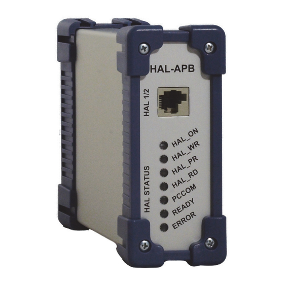
- Page 12 On, in case of communication error READY On, after power-on of board PCCOM On, in case of communication between PC and HAL- HAL_RD Telegram on VOUT HAL_PR reserved HAL_WR Telegram high level on Hall VDD HAL_ON Hall VDD on Micronas Oct. 8, 2012; APN000055_003EN...
-
Page 13: Hal Interface Connector
Sensor output V Sensor 2 OUT/DIO Fig. 3–2: Modular connector HAL1/2, front view 3.3. Firmware update The procedure for a firmware update of the HAL-APB V1.x is provided in the Applica- tion Note “Firmware Update HAL-APB V1.x” Micronas Oct. 8, 2012; APN000055_003EN... -
Page 14: Specification
In order to minimize the risk of electromagnetic disturbances, the cable should be as short as possible. Note: Especially in noisy environments beneath power switches, electromagnetic actuators, and the like, EMI-compliant layout of the wiring is mandatory. For recommended cable parameters, please refer to Table 4–6. Micronas Oct. 8, 2012; APN000055_003EN... -
Page 15: Maintenance And Calibration
Fig. 4–3: Recommended wiring - schematic sketch Table 4–6: Recommended cable parameters Symbol Parameter Min. Typ. Max. Unit Conditions Ohmic Resistance per Wire I < 10 mA Capacitance Impedance Length Micronas Oct. 8, 2012; APN000055_003EN... -
Page 16: Characteristics
Note: The voltage levels are trimmed by the manufacturer. If any of the levels listed are found to be outside the specification limits, please contact the manufacturer or the Application Support Sensors Team. The RS232 cable should be a standard serial cable. Also called straight cable. Micronas Oct. 8, 2012; APN000055_003EN... -
Page 17: Usb Driver Installation
The application note: “AN_104_FTDI_Drivers_Installation_Guide_for_WindowsXP.pdf” can be used to install the driver on a windows xp system. The application note can be either found on the Micronas Service Portal (https://service.micronas.com/workgroups/) or on the FTDI homepage. Note: Sometimes the installer repeats the whole procedure. If this happens please do the same as explained above again. -
Page 18: Board Functions
The command string has to end with <CR> (ASCII character 0x0D), optionally with <CR><LF> (ASCII characters 0x0D, 0x0A). 6.1.3. Definition of the RESPONSE Frame The response frame consists of 7...10 characters plus 1 finishing <LF> <ST>:<R9><R8>..<R2><R1><R0> <LF> ST is non-zero in case of errors (see Table 6–9) Micronas Oct. 8, 2012; APN000055_003EN... -
Page 19: Analog Measurements
(set VDD to 5 V) ftana1 (measure HAL_VDD) ftana2 (measure HAL_VOUT) = DATA / 1024 x 3 x 5V = DATA / 1024 x 5V DATA is measured by ftana command as explained in Table 7–11. Micronas Oct. 8, 2012; APN000055_003EN... -
Page 20: Error Codes
LIN interface connection Error no PWM (at PWM Duty Cycle read command) reserved reserved 10 (0xA) reserved 11 (0xB) reserved 12 (0xC) reserved 13 (0xD) data read error 14 (0xE) invalid command parameter 15 (0xF) invalid command Micronas Oct. 8, 2012; APN000055_003EN... -
Page 21: Board Mode Settings
Mode Description HAL 2810 – LIN Mode HAL 283x/50 – Biphase via DIO- Pin HAL 1820 – Biphase via V HAL 24xy – Biphase via V HAL 3625 – Biphase via V HAL 3675 – Biphase via V HAL 38xy – Biphase via V HAL 24xy –... - Page 22 (defaul=0x03E8) return value: <ST>:00000 measure V ftana1 ftana1 "\n" return value: <ST>:000000 measure the supply voltage with HAL- APB’s ADC Example => ftana1 <= 0:00177 0x00177 = 375(dec) * 15 / 1024 = 5.49 V Micronas Oct. 8, 2012; APN000055_003EN...
- Page 23 Available with firmware versions greater then 2.32. With firmware versions less then 2.32 this command is only available in mode 9. <ST> = Board Status character see from Section 6.1.5 on page 20 onwards for details Micronas Oct. 8, 2012; APN000055_003EN...
- Page 24 Application Board HAL-APB V1.x 8. HAL 1820 The HAL 1820 is a universal magnetic field sensor with a linear output, based on the Hall effect. Magnetic field, perpendicular to the branded side of the sensor provides a output voltage direct proportional to the applied magnetic flux through the Hall plate and proportional to the supply voltage (ratiometric behavior).
- Page 25 One Acknowledge if a register is written (except the NVPROG register) Detail B space space prog OUT-Pin Analog Output 2nd Acknowledge only if the NVPROG register is written and the erasing or programming was successful Micronas Oct. 8, 2012; APN000055_003EN...
- Page 26 Supply Voltage for Low Level SUPL during Programming through Sensor V Supply Voltage for High Level SUPH during Programming through Sensor V Detail B Time before and after acknowl- space s_bbit edge Acknowledge time s_bbit Programming time prog Micronas Oct. 8, 2012; APN000055_003EN...
- Page 27 A command error occurs when the command is either unknown or the execution has failed. In case of an error, the sensor transmits no acknowledge nor a body. If the protocol is understood an ACK is sent no matter if the command can/may be processed Micronas Oct. 8, 2012; APN000055_003EN...
- Page 28 “1”s, the parity bit has to be “1”. In the case of on odd number of “1”s, the parity bit has to be “0”. With the parity bit, global parity is always even. Micronas Oct. 8, 2012; APN000055_003EN...
- Page 29 HAL1820, HAL24xy, HAL28xy, HAL36xy, HAL38xy APPLICATION NOTE Application Board HAL-APB V1.x 8.5. HAL 1820 - Board commands Note: For general board commands see Table 7–11 on page 21 Table 8–14: HAL 1820 - Board commands Action Command Parameter Data write data to address xxwSTR STR = <A1><A0><D3><D2><D1>...
- Page 30 “0” (erase command) the the “1” (set command). Note: It is possible to read the registers of the HAL 1820 after locking. Changing of the memory after locking is not possible. Micronas...
- Page 31 The serial telegram is used to transmit the EEPROM content, error codes and digital values of the magnetic field from and to the sensor. bbit bbit logical 0 bbit bbit logical 1 Fig. 9–1: Definition of logical 0 and 1 bit Micronas Oct. 8, 2012; APN000055_003EN...
- Page 32 CRC: CRC bit Communication via V -Pin (Biphase-In = V / Biphase-Out = OUT-Pin) WRITE command -Pin OUT-Pin READ command -Pin OUT-Pin SUPH Detail A -Pin SUPL Detail B space space prog OUT-Pin analog output Micronas Oct. 8, 2012; APN000055_003EN...
- Page 33 (always 0) CRC: CRC bit Communication via Out-Pin / Bidirectional on Out-Pin WRITE command OUT-Pin READ command OUT-Pin Detail B space space prog OUT-Pin Analog output Detail C OUT-Pin overc switch overc Micronas Oct. 8, 2012; APN000055_003EN...
- Page 34 Time to switch sensor from appli- switch cation mode into programming mode Over current threshold +/-10 Note: Only with programming via OUT-Pin is it possible to connect and program two sensors to the same V same GND line. Micronas Oct. 8, 2012; APN000055_003EN...
- Page 35 For read command, the CRC result is calculated of data bits only (16). The polynomial for the CRC calculation is always X +X+1. In case of correct command detection (parity, CRC and command address if applicable), an ACK is sent as an answer. Micronas Oct. 8, 2012; APN000055_003EN...
- Page 36 The sensor is detecting protocol errors and command errors. The sensor is detecting following communication errors: – invalid parity – invalid checksum – command error A command error occurs when the command is either unknown or the execution has failed. Micronas Oct. 8, 2012; APN000055_003EN...
- Page 37 <CRC> checksum as 1-digit hex No. <ST>:<R3><R2><R1><R0><CRC> <ST> = Status of Board (see Table 6–9 on page 20 for details) <R> received data as 4-digit hex No. Example: read address b => xxr0b <= 0:3333E Micronas Oct. 8, 2012; APN000055_003EN...
- Page 38 For the programming during product development and also for production purposes, a programming tool including hardware and software is available on request. It is recom- mended to use the Micronas tool kit for an easy product development. Note: It is not possible to write or to read a register after locking.
- Page 39 The scheduling time between frames is set to 20 ms (fixed). Note: To apply more user friendly behavior, especially for the saving of special PID settings, the calling application software should implement the preservation of the PID settings. Micronas Oct. 8, 2012; APN000055_003EN...
- Page 40 A global error flag is set if a LIN communication error, e.g. a shorted bus or a discon- nected slave has been detected. There is no certain fault confinement implemented but only this global error information. The last error information can be kept alive or reset. Micronas Oct. 8, 2012; APN000055_003EN...
- Page 41 => lsos <= <ST>:00000000 read last data return value: <ST> board status (see Table 6– <ST>:<R7><R6><R5><R4><R3><R2><R1><R0> 9 on page 20 for details) <R> received data as 8-digit hex if lsstab1: <R3>... <R0> if lsstab2: <R7>... <R0> Micronas Oct. 8, 2012; APN000055_003EN...
- Page 42 RAM layer only. The customer must verify and (if necessary) refresh the configuration data periodically. Note: Micronas recommends to lock the COM CONFIG area when the sensors are used for qualification tests and in field applications.
- Page 43 The serial telegram is used to transmit the EEPROM content, error codes and digital values of the magnetic field from and to the sensor. bbit bbit logical 0 bbit bbit logical 1 Fig. 11–1: Definition of logical 0 and 1 bit Micronas Oct. 8, 2012; APN000055_003EN...
- Page 44 (always 0) CRC: CRC bit Communication via Out-Pin / Bidirectional on Out-Pin Mode Switch startup switch sensor output OUT-Pin WRITE command s_bifsp OUT-Pin s_bresp READ command s_bifsp OUT-Pin s_bresp Micronas Oct. 8, 2012; APN000055_003EN...
- Page 45 )For POST= 0, 10 ms must be added when POST=1 and 3, 32 ms must be added when POST=2 2)For POST= 0, 10 ms must be added when POST=1, 2 or 3, 7 ms must be added Micronas Oct. 8, 2012; APN000055_003EN...
- Page 46 32 byte only. 11.4.3. Read with base address The "read with base address" telegram uses the read data frame. The sensor transmits the data of the effective address after the header has been successful received and the Micronas Oct. 8, 2012; APN000055_003EN...
- Page 47 - invalid checksum - command error A command error occurs when the command is either unknown or the execution has failed. In case of an error, the sensor neither transmits an acknowledge nor a body. Micronas Oct. 8, 2012; APN000055_003EN...
- Page 48 <A> base address as 4-digit hex No. <CRC> checksum (see Table 6–9 <ST> board status on page 20 for details) return value: <R> received data as 5-digit hex No. <ST>:<R4><R3><R2><R1><R0> Example => pxsb30006 => <ST>:000000 Micronas Oct. 8, 2012; APN000055_003EN...
- Page 49 For the programming during product development and also for production purposes, a programming tool including hardware and software is available on request. It is recom- mended to use the Micronas tool kit for an easy product development. Note: It is not possible to write or to read a register after locking.
- Page 50 The serial telegram is used to transmit the EEPROM content, error codes and digital values of the magnetic field from and to the sensor. bbit bbit logical 0 bbit bbit logical 1 Fig. 12–1: Definition of logical 0 and 1 bit Micronas Oct. 8, 2012; APN000055_003EN...
- Page 51 CRC: CRC bit Communication via V -Pin (Biphase-In = V / Biphase-Out = OUT-Pin) WRITE command -Pin OUT-Pin READ command -Pin OUT-Pin SUPH Detail A -Pin SUPL Detail B space space prog OUT-Pin analog or digital output Micronas Oct. 8, 2012; APN000055_003EN...
- Page 52 Supply Voltage for Low Level SUPL during Programming through Sensor V Supply Voltage for High Level SUPH during Programming through Sensor V Detail B Time before and after acknowl- space s_bbit edge Acknowledge time s_bbit Programming time prog Micronas Oct. 8, 2012; APN000055_003EN...
- Page 53 (always 0) CRC: CRC bit Communication via Out-Pin / Bidirectional on Out-Pin WRITE command OUT-Pin READ command OUT-Pin Detail B space space prog OUT-Pin Analog or digital output Detail C OUT-Pin overc switch overc Micronas Oct. 8, 2012; APN000055_003EN...
- Page 54 Time to switch sensor from appli- switch cation mode into programming mode Over current threshold +/-10 Note: Only with programming via OUT-Pin is it possible to connect and program two sensors to the same V same GND line. Micronas Oct. 8, 2012; APN000055_003EN...
- Page 55 For read command, the CRC result is calculated of data bits only (16). The polynomial for the CRC calculation is always X +X+1. In case of correct command detection (parity, CRC and command address if applicable), an ACK is sent as an answer. Micronas Oct. 8, 2012; APN000055_003EN...
- Page 56 The sensor is detecting protocol errors and command errors. The sensor is detecting following communication errors: – invalid parity – invalid checksum – command error A command error occurs when the command is either unknown or the execution has failed. Micronas Oct. 8, 2012; APN000055_003EN...
- Page 57 <CRC> checksum as 1-digit hex No. <ST>:<R4><R3><R2><R1><CRC> <ST> = Status of Board (see Table 6–9 on page 20 for details) <R> received data as 4-digit hex No. Example: read address 8 => xxr08 <= 0:37B75 Micronas Oct. 8, 2012; APN000055_003EN...
- Page 58 For the programming during product development and also for production purposes, a programming tool including hardware and software is available on request. It is recom- mended to use the Micronas tool kit for an easy product development. Note: It is not possible to write or to read a register after locking.
- Page 59 Section 4.3 Maintenance and Calibration added. – Section 5 USB Driver Installation changed. Micronas GmbH Hans-Bunte-Strasse 19 D-79108 Freiburg P.O. Box 840 D-79008 Freiburg, Germany Tel. +49-761-517-0 Fax +49-761-517-2174 E-mail: docservice@micronas.com Internet: www.micronas.com Micronas Oct. 8, 2012; APN000055_003EN...
Need help?
Do you have a question about the HAL 1820 and is the answer not in the manual?
Questions and answers