Advertisement
Quick Links
Triple Half-bridge DMOS Output Driver with
Serial Input and PWM Control ATA6831/ATA6832
1. Introduction
ATA6831 and ATA6832 are fully protected universal driver interfaces designed in
SMARTIS1 technology. They are used to control up to 3 different loads by a microcon-
troller in automotive and industrial applications. The ATA6831 is housed in a QFN18
4 × 4 mm package.
Each of the 3 high-side and 3 low-side drivers is capable of driving currents of up to
1A. The drivers are internally connected to form 3 half-bridges and can be controlled
separately from a standard serial peripheral data interface. Therefore, all kinds of
loads such as bulbs, resistors, capacitors, and inductors can be combined. The IC
design particularly supports the application of H-bridges to drive DC motors. The
PWM feature allows a smooth operation of DC motors and BLDC motor control. Pro-
tection against short-circuit conditions, overtemperature, and undervoltage is
implemented. Various diagnosis functions and a very low quiescent current in standby
mode open a wide range of applications. Automotive qualification referring to con-
ducted interferences, EMC, and 2 kV ESD protection gives added value and
enhanced quality for demanding up-market applications.
ATA6831 is designed to operate on junction temperatures up to 150°C. ATA6832 is
designed for high temperature applications on junction temperatures up to 200°C If
not explicit mentioned, all comments in this document for ATA6831 are valid for
ATA6832 as well.
ATA6831/
ATA6832
Driver ICs
Application Note
9120A–AUTO–01/08
Advertisement

Related Manuals for Atmel ATA6831

Summary of Contents for Atmel ATA6831
- Page 1 ATA6831 and ATA6832 are fully protected universal driver interfaces designed in Driver ICs SMARTIS1 technology. They are used to control up to 3 different loads by a microcon- troller in automotive and industrial applications. The ATA6831 is housed in a QFN18 4 × 4 mm package. Application Note Each of the 3 high-side and 3 low-side drivers is capable of driving currents of up to 1A.
- Page 2 Figure 1-1. Triple Half-bridge DMOS Output Driver with Serial Input Control ATA6831 ATA6831/ATA6832 Driver ICs 9120A–AUTO–01/08...
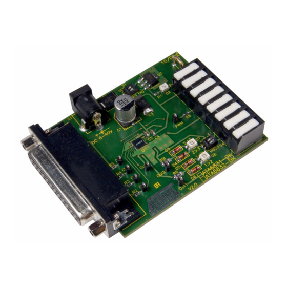
- Page 3 The core of the ATA6831-DK design kit is a PC-controlled application board. Using the ATA6831 design kit, users can easily adapt their loads via row connector pins (refer to ATA6831). The design software interface controls the design kit. The PWM input clamp allows to modulate the pace signal.
- Page 4 Figure 4-1. ATA6831-DK Application Board Schematic LM2936 200Ω BYV28 100 nF 100 nF 100 µF 10 µF MB23 MB32 MB12 MB21 ATA6831/ATA6832 Driver ICs 9120A–AUTO–01/08...
- Page 5 ATA6831/ATA6832 Driver ICs Figure 4-2. ATA6831-DK Design Kit, Application Board Component Placement; Top Side, Top View Figure 4-3. ATA6831-DK Design Kit, Application Board Top Side, Top View 9120A–AUTO–01/08...
- Page 6 Figure 4-4. ATA6831-DK Design Kit, Application Board; Bottom Side, Top View (As if PCB were Transparent) ATA6831/ATA6832 Driver ICs 9120A–AUTO–01/08...
-
Page 7: Installation
ATA6831/ATA6832 Driver ICs 5. Design Software Installation The ATA6831 design kit includes the software ATA6831. The user can also download the latest ® revision of the software from the Atmel web site, http://www.atmel.com/. Start the installation process by running the .exe file from the CD-ROM or from the downloaded file. The ATA6831.exe file is saved to a user-defined directory (for example, D:\Programs\ATA6831), and... -
Page 8: Ordering Information
Ordering Information Please contact your Atmel Sales Office or Distributor. Figure 5-2. Software User Interface ATA6831/ATA6832 Driver ICs 9120A–AUTO–01/08... - Page 9 ATA6831/ATA6832 Driver ICs Table 5-1. Functions of the Serial Interface Register Bits Input Register Function Status register reset (high = reset; the bits PSF, OPL, and SCD in the output data register are set to low) Controls output LS1 (high = switch output LS1 on)
-
Page 10: Demonstration Application
HS active to LS active or vice versa with a single programming sequence could potentially imply some shoot-through current peak across both drivers during the switching operation. The intelligent internal timing of ATA6831 guarantees that such cross- over currents are avoided. - Page 11 ATA6831/ATA6832 Driver ICs Undervoltage detection can be demonstrated with a variable power supply. As soon as the sup- ply voltage VVS falls below threshold, all activated loads are switched off, and the PSF bit in the output register is set. If the voltage returns to the normal level, the outputs switch on again to their previous setting.
- Page 12 Figure 6-1. Application with Microcontroller and Watchdog BATT BYW32 Trigger U5021M Microcontroller Reset WATCHDOG ATA6831/ATA6832 Driver ICs 9120A–AUTO–01/08...
- Page 13 The dataword intended for the last IC has to be put in first, followed by the word for the IC before and so on. In contrast to other ICs of the Atmel driver family, only a total of n shifts are needed for n ICs as any DI information is transferred immediately to the output register.
- Page 14 DI is reached after n = 3 shift operations. Figure 6-3. Daisy Chain Operation with Microcontroller and Watchdog U5021M Enable WATCHDOG ATA6831 ATA6831 ATA6831 ATA6831 Micro- controller Table 6-2. Principal Method of Shifting Datawords Through Daisy-chained ICs I/O Cycle IC number ATA6831/ATA6832 Driver ICs 9120A–AUTO–01/08...
- Page 15 ATA6831/ATA6832 Driver ICs Driving a BLDC Motor with ATA6831 The PWM capability of the ATA6831 allows to run BLDC motors, see Figure 6-4. For detailed information see Application note http://www.atmel.com/dyn/resources/prod_documents/doc4987.pdf Figure 6-4. BLDC Motor Control Application Battery BLDC Motor ATA6625...
-
Page 16: Thermal Considerations
Figure 7-1 shows the cooling arrangement of the ATA6831’s QFN 4 × 4 mm housing. The effect of the cooling area on the PCB can be further improved if the bottom side of the PCB is ground-plated and thermal vias are placed along the cooling area. Some care should be taken of the copper area’s planarity, in particular, any solder bumps arising at the thermal vias should... - Page 17 C1, but the quality of C1 (ESR) and any parasitic resistance can also have an impact. The recommended range of C1 is 22 µF to 100 µF. As stated in the ATA6831 datasheet, the maximum reverse current is 17A for a duration of 150 µs. The graph illustrated in Figure 8-2 shows the typical voltage and reverse current gradients for a capacitor value of 100 µF.
- Page 18 The clamping structures at the output stages limit the voltage peak and provide a path for the current after switching off. The maximum inductive shutdown energy for ATA6831 is specified as 15 mJ. This value applies for both low-side and high-side outputs. The energy, WL, stored in the inductor L during the switched-on state can be calculated using the following formula: ×...
- Page 19 40V is exceeded, damaging the IC. ATA6831, therefore, features a discharger circuit that prevents such unwanted effects. If V exceeds a threshold value of approximately 27V, the blocking capacitor is discharged via an integrated resistor until V falls again below the threshold.
- Page 20 Disclaimer: The information in this document is provided in connection with Atmel products. No license, express or implied, by estoppel or otherwise, to any intellectual property right is granted by this document or in connection with the sale of Atmel products. EXCEPT AS SET FORTH IN ATMEL’S TERMS AND CONDI- TIONS OF SALE LOCATED ON ATMEL’S WEB SITE, ATMEL ASSUMES NO LIABILITY WHATSOEVER AND DISCLAIMS ANY EXPRESS, IMPLIED OR STATUTORY...
Need help?
Do you have a question about the ATA6831 and is the answer not in the manual?
Questions and answers