Advertisement
Quick Links
BYOC Digital Echo & Ping Pong Kit
Instructions
Parts Checklist.................................................page 2 - 3
Populating the Circuit Board...............................page 4 - 11
Assembly........................................................page 12 - 13
Wiring the jacks, footswitch, and battery snap......page 14
Mounting the PCB....................................................page 15 - 17
Wiring the PCB................................................page 18
Finish up.........................................................page 19
Please read through the instructions completely before
beginning this project. This is one of our most difficult kits
and it is a little different than other BYOC kits, so even if you
are an experienced builder, take the time to look these
instructions over...particularly the beginning of "populating
the PCB" and "wiring the jacks, footswitch, and batterysnap".
Copyright 2008 Build Your Own Clone
Advertisement

Summary of Contents for BYOC Digital Echo & Ping Pong Kit
-
Page 1: Table Of Contents
Please read through the instructions completely before beginning this project. This is one of our most difficult kits and it is a little different than other BYOC kits, so even if you are an experienced builder, take the time to look these instructions over...particularly the beginning of “populating... -
Page 2: Parts Checklist
Parts Checklist for BYOC Digital Echo & Ping Pong Kit Resistors: 1 - 100ohm (brown/black/black/black/brown)only use this resistor if you want dedicated 18v operation 1 - 470ohm (yellow/purple/black/black/brown) 6 - 1k (brown/black/black/brown/brown) 2 - 4.7k (yellow/purple/black/brown/brown) 17 - 10k (brown/black/black/red/brown) - Page 3 2 - B100k linear 2 - B50k linear Hardware: 1 - drilled enclosure w/ 4 screws 1 - byoc pingpong kit circuit board 1 - 3pdt footswitch 4 - knobs 1 - AC adaptor jack 2 - ¼”stereoenclosed jack...
-
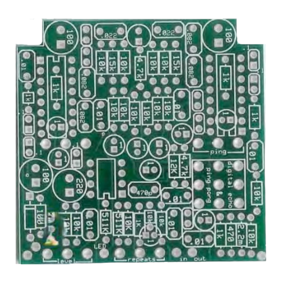
Page 4: Populating The Circuit Board
Populating the Circuit Board Before you begin: Be aware of a few peculiarities with this particular kit. There are two resistors that stand on end rather than laying flat and one that will need to be omitted and jumpered if using 9v. These three are highlighted here in yellow. There are three aluminum electrolytic caps that get mounted on the underside of the PBC highlighted here in red. - Page 5 Step 2: Omitt the 100ohm resistor if you will be using 9v. Only add the 100ohm resistor if you want dedicated 18v wall adaptor operation. If you do want dedicated 18v operation, add the 100hm resistor. If you do not want dedicated 18v operation, you must replace the 100ohm resistor with a jumper. You can use some of the component clippings left over from the last step.
- Page 6 Step 4: Add the diode. The end with the stripe(cathode) goes in the square solder pad. The end with no stripe(anode) goes in the round solder pad.
- Page 7 Step 5: Add the IC sockets. Be sure to match up the end of the socket with notch to the layout printed on the PCB with a notch. Your DIP16 sockets may not seat perfectly if you used too much solder on the 1uf caps that went on the underside of the PCB or didn't clip off enough of the excess lead.
- Page 8 Step 7: Add the .1uf tantalum capacitors. Tantalum capacitors are polarized. The positive side will have avery small “+” symbol printed on the capacitor and should go in the square solder pad. Step 8: Add the remaining seven 1uf aluminum electrolytic caps. Remember that they are polarized and the positive end goes in the square solder pad.
- Page 9 Step 9: Add the four .0022uf film caps (small green caps) highlighed in yellow and the one 47pf ceramic disc cap(small round orange cap) Step 10: Add remaining fourteen film caps (yellow box caps) highlighted in yellow and the one 470pf ceramic disc cap (highlighted in orange)
- Page 10 Step 11: Add the larger aluminum electrolytic capacitors. Remember that these are polarized and the positive end with the longer lead goes in the square solder pad.
- Page 11 Step 12: You should have two resistors left - a 1k and a 10k. These need to be mounted vertically. They are not polarized, so it does not matter which end goes where.
-
Page 12: Assembly
Assembly 1. Install the jacks first. If you are looking down inside the enclosure, the out jack goes on the right side and the in jack goes on the left. Place the washer on the outside of the enclosure. Use a 1/2" wrench to tighten. Orient the jacks so that if you are looking at the solder lug end of the jack, the bevelled “sleeve”... - Page 13 2. Install the AC adaptor jack. The bolt goes on the inside. Use a 3/4" or 14mm wrench to tighten 3. Install the potentiometers so that the solder legs are facing towards the “footswitch side”. The washers go on the outside. Use a 10mm wrench to tighten but only snug. Do not over tighten the pots.
-
Page 14: Wiring The Jacks, Footswitch, And Battery Snap
Wiring the jacks, footswitch, and battery snap Because it's a little difficult to get to the solder lugs of the enclosed style jacks once the circuit board is mounted, it's a good idea to wire this portion of the build and leave the ground and +V wires loose before mounting the PCB. -
Page 15: Mounting The Pcb
Mounting the Circuit Board Step1: Understand that the LED, potentiometers, and toggle switch will be mounted and soldered directly to the underside of the PCB. If your pots have covers, remove them before continuing. You might have to cut a slit in the cover with a blade and use a small screwdriver to get leverage. You should do the actual soldering on the topsid of the PCB. Read through all the steps in this portion before doing anything so that you can get the “big picture”. - Page 16 Step 3: Now mount the PCB with LED onto the leads of the potentiometers and toggle switch. This move may take a little finess. It's best to leave them somewhat losely mounted to the enclosure so that you can easily move them to line up with the eyelets on the PCB.
- Page 17 Step 6: Solder the LED, toggle switch, and pots on the top side of the PCB. Clip the excess LED leads. Do not clip the leads of the pots.
-
Page 18: Wiring The Pcb
Wiring the PCB... -
Page 19: Finish Up
Finishing Touches Install the chips. NOTE: The PT2399 chip will likely have a “dot” on one end that is not a marker that should be used for orienting the chip. Refer to the u-shaped notch when orienting the chip. The DIP8 dual op amp may have a u-shaped notch, a dot in one corner, or both for orienting. -
Page 20: Schematic, Understanding The Circuit And Troubleshooting
Schematic, Understanding the Circuit, and Trouble shooting Checking your wiring 1. NO POWER: If you have a completely dead pedal and your LED will not light up, this is usually a good sign that you are not getting power to the circuit. First you need to make sure that you are using a fresh battery or good power supply. - Page 21 2. NO BYPASS: Set your DMM to test for continuity. Touch the probes to the “A” locations which would be the TIPS of the 1/4” jacks. When your footswitch is in the bypass state, you should have continuity between the two “A” locations. Test lugs 8 and 9 of the footswitch for continuity.
- Page 23 Checking your PCB Ok..So Now you know bypass is working, signal is getting to and from the PCB, and that the PCB also has a connection to +9V and ground. If you're still haveing trouble, it's time to check your work on the PCB. Keep in mind that the PCB is simply a means of connecting one component or wire to another component or wire.
- Page 24 2. Check all Full Positive Voltage connections. The term “Full Positive Voltage” is used, because after D1 and R33, the voltage will be slightly diminished. Your positive voltage may be 9V at “RED” location 1, but drop to 8.5V at location 2, and then drop again to 8.2V at location 3.
- Page 25 3. Test all Half Positive Voltage “ORANGE” locations. This reading should be approx. half of what your Full Positive Voltage is after RED3. 4.5V to 4V is to be expected. Set your DMM to read 5VDC. Touch the black probe to the sleeve of either jack. Touch the red probe to the various “ORANGE”...
- Page 26 4. Test the Regulated 5V power supply. This is the power supply provide by the 78L05. 5 volt regulator. Touch the black probe to ground. Touch the red probe to the various GREEN locations. They should all be approximately 5V.
- Page 27 5. Test the dry audio signal path. Do this using a Signal Test Probe. If you look at the schematic, you'll see that “BLUE” locations 1 - 28 make up your direct dry audio signal path in order between the INPUT of the circuit and the OUTPUT of the circuit. If you are getting no sound at all when the pedal is engaged, then this is the first place you need to look.
- Page 28 6. Test the wet signal path A with the signal test probe. PURPLE 1 - 22 is signal path of the wet delayed signal from the output of the first delay chip to the input of the second when the pedal is in normal echo mode, not pingpong mode. If the first delay chip is receiving dry signal to PIN16, but is not producing a delayed signal at PIN14, then there is a problem with the chip.
- Page 29 7. Test the wet signal path B with the signal test probe. BROWN 1 - 19 is the signal path of the wet delayed signal from the output of the second delay chip to the R5/R6 junction where the wet and dry signals are mixed together before entering the output buffer when the pedal is in normal echo mode, not pingpong mode.
- Page 30 7, but the outputs of both chip A and Chip B are being looped back in parallel into the input of chip B rather than the output of A and B in series being looped back into A. For high-resolution color map, visit: http://byocelectronics.com/pingpongcolormapscheme.pdf ©2008 byoc, LLC...
Need help?
Do you have a question about the Digital Echo & Ping Pong Kit and is the answer not in the manual?
Questions and answers