Table of Contents
Advertisement
Advertisement
Table of Contents

Summary of Contents for Brandywine PMC-SYNCCLOCK32-UNIV
- Page 1 (217) 352-9330 | Click HERE Find the Brandywine Communications / JXI2 PMC-SyncClock32-UNIV at our website:...
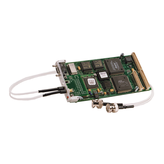
- Page 2 PMC-SYNCCLOCK32-UNIV Synchronized Clock with 32 bit PCI 3.3V or 5V Signaling Interface Operation & Maintenance Manual 13 JUNE 2005 Document No. 8004200 Module S/N A L A H/W Rev Level:B6 Options: -TAG3IRS422-HQ-10OPPSPW422- PTTIIN-NORDEN2-1TR-CONFCOAT jxi2, Inc. 10432 Brian Mooney Ave. El Paso...
- Page 3 Manual Addendum for -HQ -10OPPSPW422-PTTIIN-NORDEN2 options The PMC-SYNCCLOCK32 module shipped with this manual has the -HQ, -100PPSPW422, -PTTIIN, and — NORDEN2 options installed. The -HQRS422 option provides for use of Havequick II serial and 1 PPS time reference per ICD-GPS-060A, The input pin assignments are: 1PPS /GND: J3 pin 14 /GND: J3 pin 32...
- Page 4 -TAG3IRS422 Option Manual addendum The —TAG3IRS422 option provides a total of 3 external event time tags with RS422 inputs level terminated in 100 ohms compared with only one single ended TTL level input on the standard PMC-SYNCCLOCK32. Each of the 3 external time tags has its' own polarity (r or e d g e ) and its' own interrupt enable.
- Page 5 I I " t 8 i m o n o . c 4 s e p 0 4 j c k m a s k o f f h i n i b l o f E x t n C t l S t s P o r t i n R d y t e s t / * t 8 i m o n o .
- Page 6 i f ( ( s u b s y s i d v i d ! = 0 x 1 0 4 2 1 0 b 5 ) 1 1 ( a n y 9 0 5 0 _ 1 0 b 5 ! = 0 ) ) { p r i n t ! ( "...
- Page 7 I I / / T 3 I T I N T R . 0 7 J U L 0 6 J C K e v t 2 t o e v t 0 s p a c i n g c h a n g e d t o 6 m s e c / / T 3 I T I N T R .
- Page 8 r e g s . h . a 1 = 0 x 0 2 ; r e g s . w . c x = 0 x 9 0 5 0 ; r e g s . w . d x = 0 x 1 0 b 5 ; / * q u e r y i f d e v i c e i d 9 0 5 0 / v e n d o r i d 1 0 b 5 i s p r e s e n t * / r e g s .
- Page 9 + b i n ( ( o l d t l o » 2 4 ) & 0 x 0 f f ) * 1 0 0 0 0 0 0 + b i n ( ( o l d t l o » 1 6 ) & 0 x 0 f f ) * 1 0 0 0 0 + b i n ( ( o l d t l o »...
- Page 10 " v o i d i n t e r r u p t f a r p c _ i n t ( v o i d ) / * H a n d l e e x t e r n a l e v e n t i n t e r r u p t s * / i n t —...
- Page 11 Manual Addendum for -HQ -10OPPSPW422-PTTIIN-NORDEN2 options The PMC-SYNCCLOCK32 module shipped with this manual has the -HQ, -10OPPSPW422, -PTTIIN, and — NORDEN2 options installed. The -HQRS422 option provides for use of Havequick II serial and 1 PPS time reference per ICD-GPS-060A, The input pin assignments are: 1PPS /GND: J3 pin 14 /GND: J3 pin 32...
- Page 12 Manual Addendum —ITR-CONFCOAT options The PMC-SYNCCLOCK32 module shipped with this manual has the —ITR and -CONFCOAT options installed. The —ITR option uses integrated circuits that are rated —40C to +85C. The —CONFCOAT option is conformal coating.
-
Page 13: Table Of Contents
INTRODUCTION SPECIFICATIONS Physical: Inputs & Outputs (see addenda at front of manual for custom options) Bus Interface (see addenda at front of manual for special options): PCI Configuration Registers INPUT/OUTPUT CONNECTIONS Bezel J1, J2 (SMB): Front Panel J3 (IEEE 1284 type jack): (see addenda at front of manual for custom options) PMC Bus Connector (PI/P2): PMC bus P4: (see manual front addendum for custom options) CONFIGURATION, INSTALLATION &... - Page 14 Reading Current Time (-BIN option only) Reading External Time Tags (non -BIN option) Reading External Binary Time Tags (-BIN option only) Simulating External Time Tags Heartbeat Pulses and Interrupts Dual Port RAM for Supplementary Status/Control Accessing Dual Port RAM Sending Commands through the Dual Port RAM. Setting Leap Year Control in Dual Port RAM Selecting 1PPS or Time Code Reference Priority in Dual Port RAM Setting Time Code Propagation Delay Polarity in Dual Port RAM...
- Page 15 SCHEMATIC DRAWINGS PARTS LIST PROGRAM LISTINGS...
-
Page 16: Introduction
10 MHz crystal oscillator. The user program can specify the propagation delay from the time code source to the PMC or the 1 PPS source to the PMC-SYNCCLOCK32-UNIV input and the PMC-SYNCCLOCK32-UNIV will automatically adjust the clock to compensate for the delay. A redundancy feature allows BOTH a 1 PPS signal and a time code to be used as references. -
Page 17: Specifications
SPECIFICATIONS Physical: Dimensions: 74 mm X 149 mm ("Single CMC") Power: +5V ±5% .12A typ, .15A max +3.3V±5% .12A max +12V± 5%: .06A typ .10A max -12V± 5%: .025A typ .05A max Fabrication: 1.68mm±.2mm (.062 in±008in) FR4, 6 layer Temperature: 0 to 70C operating, -40C to 85C storage -40C to +85C operating with —ITR option Humidity:... -
Page 18: Bus Interface (See Addenda At Front Of Manual For Special Options)
Bus Interface (see addenda at front of manual for special options): PCI memory space (8 contiguous longwords) Addressing: I NTA Interrupt levels: Register Assignments: Read Usage Usage Offset from B i t s Base Addr B i t 0 is <31:0>... -
Page 19: Pci Configuration Registers
PCI Configuration Registers Default values in italics EEPROM initialization values in bold EEPROM Bits <31:24> B i t s <23:16> B i t s <15:8> B i t s <7:0> PCI Writeable PCI CFG Writeable register address Device ID 9030 Status 0002 Y(<31:8>) -
Page 20: Input/Output Connections
INPUT/OUTPUT CONNECTIONS Bezel J1, J2 (SMB): J1 is used for modulated time code input. J2 (optional) is used for modulated time code output (option). Front Panel J3 (IEEE 1284 type jack): (see addenda at front of manual for custom options) Pin 1: Time Code Input ("+"... -
Page 21: Pmc Bus Connector (Pi/P2)
Pinouts for L-COM CSM84CC-1M,-2M,-3M,-5M,-10M cables: J3 signal wire color J3 pin J3 pin wire color J3 signal CODEIN+ 19 BLU/WHT CODEIN- PPSIN+ 20 YEL/BLK PPSIN- 21 BRN/WHT G N D GPSRXI- 22 RED/BLK GPSRXI- GPSRXO+ 23 GRN/BLK GPSRXO- RTCMIN+ 24 ORG/BLK RTCMIN- DCCODEIN+ PNK/RED 25 PNK/BLU DCCODEIN-... - Page 22 PMC bus P4: (see manual front addendum for custom options) Pin 1: CLK1: HEARTBEAT user programmable pulse output Pin 3: CLKO: Low rate (50 PPS ...00153 PPS) user programmable pulse output Pin 5: CLK2: High rate (1.5 M PPS to 45.7 PPS) user programmable pulse output Pin 6: Pin 7: Time tag input TTL level Pin 9: "REF"...
-
Page 23: Configuration
Installation Double check and record configuration settings before installing the PMC-SYNCCLOCK32. The PMC host system should be powered down before the PMC-SYNCCLOCK32-UNIV is added. Plug the PMC-SYNCCLOCK32-UNIV into the appropriate location in the PMC host. Attach inputs and outputs before applying power . -
Page 24: Pci Address/Irq Configuration Verification (X86 Systems)
PMC-SYNCCLOCK32-UNIV is Big Endian while the PCI bus is little Endian. So, the PCI memory space base address is 01010200. Now, the PCI I/O address range 0000000-3EFFFFFis mapped to MVME 1600-001 address space C0000000-FEFFFFF. So in this example, the PMC-SYNCCLOCK32-UNIV base address is C1010200 in MVME1600- 001 POWER-PC address space. -
Page 25: Led Status Indication
LED Status Indication LED1 (red LED) flashes echo the data in the DP_Extd_Sts dual port RAM location. The LSB (DP_Extd_Sts Nosync) is sent first. "0" bits are short flashes, "1" bits are long flashes. Trailing short flashes are deleted. For example, if DP_Extd S t s is 1C, the pattern is short short long long long. -
Page 26: Programming
PCI bus addresses. The DPDEF .H file contains the Dual Port RAM assignments. The REGDEF .H file contains the offset addresses and bit assignments for registers. Note that all accesses to the PMC-SYNCCLOCK32-UNIV are relative to a BASE address, which varies depending on the user environment. -
Page 27: Accessing Pmc-Syncclock In Windows Environment
Accessing PMC-SYNCCLOCK in Windows environment In a Windows environment, a thread calls SelectSyncclock once to get the virtual base address of the PMC-SYNCCLOCK in user space: u n s i g n e d l o n g B A S E = - 1 ; HANDLE H a n d l e ;... -
Page 28: Reading Current Time (Bcd Format) (Non -Bin Option)
Reading Current Time (BCD Format) (non -BIN option) The first read operation (from register B A S E + S e c l O _ U s e c l _ P o r t latches all the other current time bits at s a m e time. -
Page 29: Reading External Time Tags (Non -Bin Option)
RAM DP E x t d S t s location. Reading External Time Tags (non -BIN option) The simplest and fastest way to read external time tags uses the PMC-SYNCCLOCK32-UNIV external time tag latches which may be read directly across the PCI bus: Example: Reads all 8 bytes of external BCD time tag with two C statements that take about 2 usec to execute on a 350 MHz AMD K6 / Windows 98. -
Page 30: Reading External Binary Time Tags (-Bin Option Only)
90 milliseconds after the time tag occurs. Reading External Binary Time Tags (-BIN option only) The simplest and fastest way to read external time tags uses the PMC-SYNCCLOCK32-UNIV external time tag latches which may be read directly across the PCI bus:... -
Page 31: Heartbeat Pulses And Interrupts
The heartbeat rate may be changed using the dual port RAM. Dual Port RAM for Supplementary Status/Control A 256 byte dual port RAM on the PMC-SYNCCLOCK32-UNIV shares access between the microprocessor in the PMC-SYNCCLOCK32-UNIV and the host PCI computer. The first 128 locations are READ ONLY from the user program. -
Page 32: Sending Commands Through The Dual Port Ram
Selecting 1PPS or Time Code Reference Priority in Dual Port R A M The PMC-SYNCCLOCK32-UNIV allows redundant use of a time code input and a 1 PPS (or GPS receiver) input simultaneously as reference. The DP_Control O_CodePriority bit of the DP_Control 0 dual port RAM location will be "1"... -
Page 33: Setting Time Code Propagation Delay Polarity In Dual Port Ram
Specifying Modulated Input Code Format in Dual Port R A M The PMC-SYNCCLOCK32-UNIV allows the user to specify the format of the modulated input time code in the DP_Code_Select dual port RAM address by writing the following constants defined in DPDEF.H. -
Page 34: Setting Time Code Propagation Delay In Dual Port Ram
For achieving µsecond accuracy it is necessary for the user to set the propagation delay correction for each PMC-SYNCCLOCK32-UNIV installation. The correct values for propagation delay correction can be estimated base on cable lengths and propagation speed of the cable used, but the effects of capacitive loading usually require that the 10s and units of µsecond digits... -
Page 35: Changing Heartbeat, Lowrate And Rate2
Changing Heartbeat, Lowrate and Rate2 The CLKO signal (J3 pin 7), the Heartbeat signal (J3 pin 8), and the CLK2 signal (J3 pin 5) are generated by three sections (0,1, and 2 respectively) of a programmable 82C54 clock IC. Each section divides an input signal by a programmable divisor of 2-65535. The input signal for section 0 is a 100 PPS pulse synchronized to the clock. -
Page 36: Gps Satellite Tracking And Navigation Data (Except Have-Quick Receivers)
"Hardware Triggered Strobe" . Seldom used. Output is high until D P _ c t i _ m o d e S jam sync. Then after count=0 output goes low one CLKx cycle and then goes high again. Bit <5:4> should always be 11 ("DP_ctl rw") Bit<7:6>: Bit value Mnemonic... -
Page 37: Differential Data Acknowlege Count (-Df Option With Motorola Oncore Only)
Differential Data Acknowlege Count (-DF option with Motorola Oncore Only) The Motorola Oncore GPS receiver sends the on-board Z80 microprocessor an acknowledge message whenever a valid RTCM104 message has been successfully received. The Z80 firmware will increment the dual port RAM DP GPS_RTCM_Ack location whenever an acknowlegement is received from the Oncore. -
Page 38: Theory Of Operation
Theory of Operation MINL • Z80 Microprocessor OPTIONAL Time Code MINL F P G A TRANS- Strip CODEEDGE CODEEDGE FORMER I R I G D C O U T write • 1 PPS Modulated IN R A M BUFFERED Code Gen FPGA REFERENCE 1 PPS LOW 28TIME LATCH... -
Page 39: Voltage Divider
Voltage Divider The analog reference signal swinging + and - around +5 V is applied to one end of voltage divider R5 and R6. The other end of the divider is +5 volts. Because R6 is about twice the value of R5, the peak to peak AC voltage at the R5/R6 junction will be 2/3 the peak to peak AC voltage at C1 + side - but still centered on +5 V. -
Page 40: Clock Conditioning
PMC-SYNCCLOCK32-UNIV against transients if an external oscillator is used. C28 AC couples the sine wave and R13/R14 provide hysterisis. CR2 and CR3 provide protection. -
Page 41: 3.0 M H Z Frequency Generation
3.0 M H z frequency generation 3.0 MHz synchronous to the main clock is output by the FPGA for use in generating "modem" rates 24000 Hz, 2400 Hz etc. that are not easily derived from 10 MHz or 5 MHz. The 3 MHz is disciplined by the same mechanisms used for the FPGA clock, so it will be synchronous to the FPGA clock. - Page 42 by U1 which immediately terminates with a PCI bus specification V2.1 retry to release the PCI bus. Then U1 completes the access over the local bus and completes the user access with a PCI retry cycle.
-
Page 43: Board Layout
N M 11•11 11111 11111 1111111 11111 11111 I N N N M 1 1 1 1 111111 • ' i - I l l r � t l : i n " g r t t - - P 1 L � J r \ - - - / e "... - Page 44 • IMO I I I I I I I 7 MEN I Mini 6 M N 1•1113 M I FRONT PA N E L I / O V+ + 1 2 V P2)1 TRST* TCK P 1 ) I CODEIN+ J 3 1 C O D E I N - 1 9 V- - 1 2 U P 1 ) 2 I N TA * I N T A *...
- Page 45 ri e ir " ' I MIS M I N I 111111 + 3 . 3 1 H L 9 0 3 0 e 1 9 0 3 ( i _ + 3 . 3 4 5 A D 1 1 8 3 L D 1 1 + 3 .
- Page 46 1 1E13 1 = 1 I 1=1 21E1 I 11111 61E11 110 EP INSTALL R 4 4 T O D I S A B L E R 4 4 R 4 5 U12 2 8 4 C 4 4 6 ROM PORTION O F U 4 WHEN USING EMU O R 6 ) 6 3 6 1 3 RXDA...
- Page 47 M N M I N ME! 7 M I 1 M N 611111I U17 5 7 8 1 - 0 5 1 OUT I N _ L 3 4 GND GND - - 1UF • - = . GND GNO . g . 4 N / C N / C '''' 100K NJM2082...
- Page 48 B I L L O F M AT E R I A L S P M C - S Y N C - U N I V - I T R - T 3 I - H Q - P I T I - 1 0 0 P P S 4 2 2 R E V B 6 T h u O C t 1 2 1 0 : 0 3 : 5 3 2 0 0 6 QTY J X N D E S C R I P T I O N R E F .
- Page 49 B I L L O F M AT E R I A L S P M C - S Y N C - U N I V - I T R - T 3 I - H Q - P T T I - 1 0 0 P P S 4 2 2 R E V B 6 T h u O c t 1 2 1 0 : 0 3 : 5 3 2 0 0 6 I I Q T Y J X N D E S C R I P T I O N R E F .
- Page 50 I / / t 8 i r e g s . h 1 3 J U N 0 5 J C K d o c u m e n t l O O n s e c d i g i t e x t t i m e t a g r e a d / * T 8 I R E G S .
- Page 51 I I # d e f i n e E x t 7 Y e a r l M i n l P o r t 0 x 7 c / * L O N G R O e x t . t i m e t a g 7 l O s e c . . 1 0 m s e c * /...
- Page 52 I I / * R E G D E F. H 5 S E P 0 3 J C K F I X COMMENT O N E x t P o l a r i t y : 0 = ' , 1 = V * / / * R E G D E F.
- Page 53 / * D P D E F. H 1 0 J A N 0 3 J C K a d d D P C o n t r o l O : I g n o r e P P S & I g n o r e C o d e d e f i n i t i o n s / * D P D E F.
- Page 54 0 x 9 1 M a j o r t i m e 1 0 , 1 m i n u t e * / # d e f i n e DP M a j o r T i m e m l 0 m 1 # d e f i n e DP M a j o r —...
- Page 55 3 a d d GPS c o m m a n d s f o r o p e n , s h o r t b i t s i n R c v r S t a t u s M 1 2 * / / * g p s d e f .
- Page 56 0 x 2 c 4 b y t e c h a n n e l 3 i n f o I I # d e f i n e D P G P S C H 3 4 i n f o # d e f i n e D P G P S C H 4 0 x 3 0 4 b y t e c h a n n e l...
- Page 57 f l a g * / # d e f i n e D P G P S R c v r S t a t u s I n s V i s i b 0 x 0 2 / * I n s u f f i e n t v i s s a t s * d e f i n e D P G P S —...
- Page 58 / * c u r t i m e . c 2 1 f e b 2 0 0 3 d i s p l a y c u r r e n t t i m e f r o m p c i - s y n c c l o c k a s 2 8 d i g i t l o n g w o r d * C o p y r i g h t ( c ) 2 0 0 2 P L X T e c h n o l o g y , I n c .
- Page 59 / * m a t t s t . c p p 2 1 f e b 2 0 0 3 j c k t e s t s M a t c h f u n c t i o n f o r P C I - S Y N C C L O C K * C o p y r i g h t ( c ) 2 0 0 2 P L X T e c h n o l o g y , I n c .
- Page 60 / * d p d u m p . c 2 1 f e b 2 0 0 3 j c k d e m o n s t r a t e s e l e c t i n g s y n c c l o c k a n d r e a d i n g d u a l p o r t R A M * C o p y r i g h t ( c ) 2 0 0 2 P L X T e c h n o l o g y , I n c .
- Page 61 / * s e t m a j o r . c 2 2 f e b 2 0 0 3 j c k s e t SYNCCLOCK m a j o r t i m e * C o p y r i g h t ( c ) 2 0 0 2 P L X T e c h n o l o g y , I n c . * P L X T e c h n o l o g y I n c .
- Page 62 I I / * h e a r t . c p p 2 2 f e b 2 0 0 3 j c k d e m o c h a n g i n g SYNCCLOCK h e a r t b e a t r a t e * C o p y r i g h t ( c ) 2 0 0 2 P L X T e c h n o l o g y , I n c .
- Page 63 / * g p s b i n . c 7 m a r 2 0 0 3 d i s p l a y GM G P S l a t / l o n / h e i g h t d a t a * C o p y r i g h t ( c ) 2 0 0 2 P L X T e c h n o l o g y , I n c .
- Page 64 c h a r s t a t u s ; * ( v o l a t i l e u n s i g n e d c h a r * ) (BASE+Dual P o r t A d d r e s s P o r t ) = a d d r ; c h a r * ) ( B A g E + S t a t u s _ P o r f ) ;...
Need help?
Do you have a question about the PMC-SYNCCLOCK32-UNIV and is the answer not in the manual?
Questions and answers