Advertisement
Quick Links
Advertisement

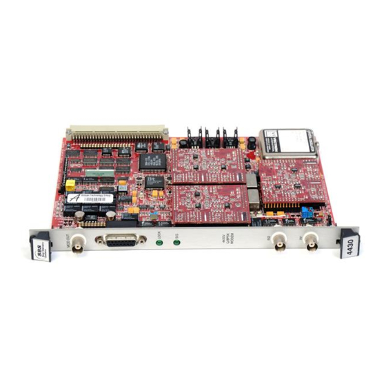
Summary of Contents for SBS Technologies 4430-V BPSK VME
- Page 1 Artisan Technology Group is your source for quality new and certified-used/pre-owned equipment SERVICE CENTER REPAIRS WE BUY USED EQUIPMENT • FAST SHIPPING AND DELIVERY Experienced engineers and technicians on staff Sell your excess, underutilized, and idle used equipment at our full-service, in-house repair center We also offer credit for buy-backs and trade-ins •...
- Page 2 Optional Modulator User’s Manual 1: Introduction ............1 2: Installation ............11 3: Programming Information ......21 A: Revisions ............71 SBS Technologies® 7401 Snaproll NE Albuquerque, NM 87109 Sales: 800-SBS-1553 or 505-875-0600 Fax: 505-875-0400 Tech Support: 877-832-4727 Tech Support Email: support.government@sbs.com Documentation Support Email: govdocs@sbs.com...
- Page 3 This manual, as well as the software described herein, is furnished under license and may only be used or copied in accordance with the terms of such license. SBS Technologies and the SBS logo are trademarks of SBS Technologies, Inc. All other brand names and product names contained herein are trademarks, registered trademarks, or trade names of their respective holders.
-
Page 4: 1: Introduction
Introduction 1: Introduction General 1.1.1 Description The Model 4430-V and the 4430-VN VME cards are high-performance tunable BPSK/QPSK demodulator modules for the VMEbus. The demodulator features a tunable input carrier frequency range of 6kHz to 6 MHz. A tunable modulator is available for the Model 4430-V &... - Page 5 4430-V & VN BPSK/QPSK VME Demodulator & Optional Modulator User’s Manual Contents of Getting Started with the 4430-V & VN This manual is intended to assist you in getting the 4430-V & VN up and run- ning as quickly as possible. It addresses the following: ➢...
- Page 6 Introduction Conventions The following conventions appear in this document. These conventions may dif- fer from those used in other SBS publications. The subsections listed below de- scribe each convention in more detail: ➢ Typographic Conventions ➢ Words Having Special Meaning ➢...
- Page 7 4430-V & VN BPSK/QPSK VME Demodulator & Optional Modulator User’s Manual Table 1.4.2: Words with Special Meaning Word Meaning Enter Key in the specified text or variable information and press the Return key. Type Key in the specified text. Do not press Return . 1.4.3 Compound Keystrokes and Menu Selections Whenever a procedure instructs you to press multiple keys, a double angle...
- Page 8 Introduction 1.4.4 Symbols The following symbols appear throughout this manual: Warning: Paragraphs next to this symbol contain information critical to module operation or to your safety. Note: Paragraphs next to this symbol contain information important to module operation. Tip: Paragraphs next to this symbol contain useful tips. Cross Reference: Paragraphs next to this symbol contain cross references to a related page in this manual, or to other SBS publications.
- Page 9 4430-V & VN BPSK/QPSK VME Demodulator & Optional Modulator User’s Manual Block Diagrams Figure 1.5.1: 4430-V/VN Block Diagram Doc: 4430_V,VN.fm, © 11 Jul 2005, 14:55 Artisan Technology Group - Quality Instrumentation ... Guaranteed | (888) 88-SOURCE | www.artisantg.com...
- Page 10 Introduction Figure 1.5.2: 4430-V/VN QPSK Setup Diagram Artisan Technology Group - Quality Instrumentation ... Guaranteed | (888) 88-SOURCE | www.artisantg.com...
- Page 11 4430-V & VN BPSK/QPSK VME Demodulator & Optional Modulator User’s Manual Figure 1.5.3: BPSK Setup Diagram Doc: 4430_V,VN.fm, © 11 Jul 2005, 14:55 Artisan Technology Group - Quality Instrumentation ... Guaranteed | (888) 88-SOURCE | www.artisantg.com...
- Page 12 Introduction Specifications 1.6.1 Electrical Specifications Table 1.6.1: Electrical Specifications Specification Description Demodulator 6 kHz to 6 MHz Tunable. Independently tunable front end high Carrier Frequency pass and low pass filters. Data Rates To 1.5Mbps. 4430-V = 0.05% to 3% of Carrier Frequency. Loop Bandwidth 4430-VN = 0.003% to 0.05%.
- Page 13 10 4430-V & VN BPSK/QPSK VME Demodulator & Optional Modulator User’s Manual 1.6.2 System Interface Specifications Table 1.6.2: System Interface Specifications Specification Description Interface Type VME(C.1) A24 D08 Slave for setup status. Demod center frequency Modulator center frequency Data filter frequency Input LPF frequency Input HPF frequency Programmable Functions...
-
Page 14: 2: Installation
Installation 2: Installation Introduction Chapter 2 provides installation instructions for both the Model 4430-V and Model 4430-VN. If you ordered the 4430-V/VN directly from SBS for your specific application, hardware identification is straightforward. If, however, you “inherited” the board from within your own company, proper identification of the hardware as well as proper application of the board may be more difficult. - Page 15 12 4430-V & VN BPSK/QPSK VME Demodulator & Optional Modulator User’s Manual 2.2.3 Firmware Numbers Firmware identification numbers are printed on labels attached to their respec- tive programmable parts. See Figure 2.2.1 on page Figure 2.2.2 on page Figure 2.2.3 on page JP1 Jumpers DIP Switches Factory Set...
- Page 16 Installation JP1 Jumpers DIP Switches Factory Set S2 and S1 Do Not Remove Modluator Optional Q/BPSK Output Modulator Connector LED LOCK Indicator LED SIG Indicator I - Low Pass Q - Low Pass Filter Filter Demodluator Input 2 Input Low Pass Filter Demodluator Input 1...
- Page 17 14 4430-V & VN BPSK/QPSK VME Demodulator & Optional Modulator User’s Manual JP1 Jumpers DIP Switches Factory Set S2 and S1 Do Not Remove Modluator Output Connector LED LOCK Indicator LED SIG Indicator Demodluator Input 2 Demodluator Input 1 Model Number Serial JMP1 Jumpers...
- Page 18 Installation Hardware Setup 2.3.1 Hardware Revisions The nomenclature and positioning of hardware on Revision D is slightly differ- ent than on Revisions A, B and C, but does not effect setup. ➢ Rev A, B and C, without modules is shown in Figure 2.2.1.
- Page 19 16 4430-V & VN BPSK/QPSK VME Demodulator & Optional Modulator User’s Manual Configuration Information 2.4.1 Setting Interrupts The 4430-V/VN has no interrupts. 2.4.2 Jumpers The 4430-V/VN has jumpers - J1 and JP1. These are identified in Figure 2.2.1 on page 12.
- Page 20 Installation ➢ LED Lock Indicator - When this LED is illuminated, it indicates that the demodulator is locked to the signal. ➢ LED Sig Indicator - When this LED is illuminated, it indicates that there is a signal detected on selected input. 2.4.6 Optional Modules The 4430-V/VN has one optional module, an on-board modulator.
- Page 21 18 4430-V & VN BPSK/QPSK VME Demodulator & Optional Modulator User’s Manual J4 Pin-outs Connector J4 provides miscellaneous signal inputs and outputs. The pin-out is shown in Table 2.6.1, “J4 Pinouts,” on page 18. Where pairs of signal names have trailing + and – signs, these represent the pair connections of an RS-422 signal.
- Page 22 Installation Pin C32 Pin C1 Pin B32 Pin B1 Bottom Edge of Board Pin A32 Pin A1 Figure 2.6.2: P1 Pinout Interface to VMEbus Table 2.6.2: P1 Pinouts Pin # BBSY* BCLR* ACFAIL* BG0IN* BG0OUT* BG1IN* BG1OUT* BG2IN* BG2OUT* SYSCLK BG3IN* SYSFAIL* BG3OUT*...
- Page 23 20 4430-V & VN BPSK/QPSK VME Demodulator & Optional Modulator User’s Manual Mating Component Information 2.7.1 Cable Information Cable connections are custom-designed for each application. You may purchase connectors to produce your own cables, or order them from a supplier. 2.7.2 Cable Connector Figure 2.7.1...
-
Page 24: 3: Programming Information
Programming Information 3: Programming Information Host Interface The host programming interface of the 4430-V/VN maps to 128 bytes of VME address space. An array of 35 8-bit registers are located at the bottom of the ad- dress space. Writing to or reading from addresses that are not listed in the reg- ister map in Table 3.2.1, “Register Map-4430-V/VN Demodulator &... - Page 25 22 4430-V & VN BPSK/QPSK VME Demodulator & Optional Modulator User’s Manual Register Map Table 3.2.1 shows a numerical listing of interface registers for the 4430-V/VN demodulator and optional modulator. Table 3.2.1: Register Map-4430-V/VN Demodulator & Optional Modulator Physical Register Data Ref.
- Page 26 Section 3.3.2 enables you to evaluate your setup criteria to ensure that it falls within the operational capabilities of the 4430-VE. If not, you should contact your SBS Technologies representative to determine which module will best serve your needs. 3.3.1...
- Page 27 24 4430-V & VN BPSK/QPSK VME Demodulator & Optional Modulator User’s Manual If the demodulator contains the optional modulator daughter board (refer to Chapter 2 for configuration details), is the modulator being utilized? (Options: Yes or No) Modulator Select = Note: If the response to question 7 is “No,”...
- Page 28 Programming Information Therefore, perform the following calculations and determine if the results fall within the stated range: Calculate the demodulator data rate to carrier frequency ratio. (Ratio: <0.25) Demod Ratio = Calculate the modulator data rate to carrier frequency ratio. (Ratio: <0.25) Mod Ratio = 3.3.4...
- Page 29 26 4430-V & VN BPSK/QPSK VME Demodulator & Optional Modulator User’s Manual Table 3.3.1: E versus LPSR Selection Table LPSR LPSR 0.00003 0.007 0.00005 0.015 0.0008 0.02 0.00014 0.035 0.00024 0.06 0.0003 0.0006 0.15 0.001 0.002 0.004 Calculate the percentage loop bandwidth by dividing the loop bandwidth value by the demodulator carrier frequency as shown below.
- Page 30 Programming Information Note: In both cases described above, the user should be no- tified that the selected Eb/No is not directly supported. In the case that the %LBW value is outside the given range on the low side, the user should be notified that the demodula- tor can not support the signal to noise ratio selected.
- Page 31 28 4430-V & VN BPSK/QPSK VME Demodulator & Optional Modulator User’s Manual 3.3.9 Calculation of the Input Low Pass Filter Frequency To calculate the demodulator input low pass filter frequency, the demodulator carrier frequency must be added to the symbol rate multiplied by two. The fol- lowing equation applies.
- Page 32 Programming Information input signal is likely to experience a noisy environment, selection of more mod- erate Eb/No settings will allow for a wider loop bandwidth setting and more consistent operation. ➢ Eliminating loop stress during demodulator setup Loop stress can have an affect the demodulator’s tuning process. If the input to the demodulator is different than the source being applied to the input, it is best to remove stress from the input loop by switching to an unused input and then returning to the original input.
- Page 33 30 4430-V & VN BPSK/QPSK VME Demodulator & Optional Modulator User’s Manual Demodulator Quadrature NCO - Phase Accumulator Reset Repeat Step 1 through Step 10. Modulator Carrier Frequency NCO - Synchronous Mode Control 11. Modulator Carrier Frequency NCO - Asynchronous Mode Control 12.
- Page 34 Programming Information Register Programming The following subsections contain information on programming the 4430-V/ VN registers. Example calculations are included at the bottom of each register definition page. The example calculations within this report are based on the following 4430 ex- ample setup: ➢...
- Page 35 32 4430-V & VN BPSK/QPSK VME Demodulator & Optional Modulator User’s Manual Unused Unused Unused Unused Unused Unused Synchronous Mode Control Unused Figure 3.5.1: Register 08h Bit Assignments Table 3.5.1: Carrier Frequency NCO Synchronous Mode Control Register Definition Bit No. Bit Name(s) Functional Description Unused...
- Page 36 Programming Information 3.5.2 Register 18h (31h), Quadrature NCO - Synchronous Mode Control This register provides synchronous mode control of the demodulator Quadra- ture NCO. Figure 3.5.2 illustrates the breakout of register bit assignments. Prior to programming the NCO, the synchronous mode must be enabled. Unused Unused Unused...
- Page 37 34 4430-V & VN BPSK/QPSK VME Demodulator & Optional Modulator User’s Manual 3.5.3 Register 0Ah (15h), Demod Carrier Freq NCO - Asynchronous Mode Control This register provides asynchronous mode control of the demodulator Carrier Frequency NCO. Figure 3.5.3 illustrates the breakout of register bit assign- ments.
- Page 38 Programming Information 3.5.4 Register 1Ah (35h), Demod Quadrature NCO - Asynchronous Mode Control This register provides asynchronous mode control of the demodulator quadra- ture NCO. Figure 3.5.4 illustrates the breakout of register bit assignments. Prior to programming the NCO, the asynchronous mode must be enabled. Unused Unused Unused...
- Page 39 36 4430-V & VN BPSK/QPSK VME Demodulator & Optional Modulator User’s Manual 3.5.5 Register 00h, 01h, 02h, 03h (01h, 03h, 05h, 07h), Demod Carrier Freq NCO This group of registers provides the programming interface to the demodulator carrier frequency NCO. The registers are to be programmed in a group as a sin- gle 32-bit integer value.
- Page 40 Programming Information Table 3.5.5: Demodulator Carrier Frequency NCO Group Register Definition Bit No. Bit Name(s) Functional Description Most significant carrier frequency word (See Figure 31-24 Demod Carrier Frequency 3.5.5 for register assignments) Carrier frequency word 3 (See Figure 3.5.5 for register 25-16 Demod Carrier Frequency assignments)
- Page 41 38 4430-V & VN BPSK/QPSK VME Demodulator & Optional Modulator User’s Manual 3.5.6 Register 10h, 11h, 12h, 13h (21h, 23h, 25h, 27h), Demod Quadrature NCO This group of registers provides the programming interface to the demodulator quadrature NCO. The registers are to be programmed in a group as a single 32- bit integer value and should be programmed with the same values as the demod- ulator carrier frequency NCO registers.
- Page 42 Programming Information The value programmed into the registers are based on the following equation: x 214.74837 Register Value = Demod f Results are rounded to the nearest integer and then cleaved into four separate bytes as shown in Figure 3.5.6. Table 3.5.6: Demodulator Quadrature NCO Group Register Definition Bit No.
- Page 43 40 4430-V & VN BPSK/QPSK VME Demodulator & Optional Modulator User’s Manual 3.5.7 Register 0Ch (19h), Demod Carrier Freq NCO - Phase Accumulator Reset This register resets the phase accumulator for the demodulator carrier frequency NCO. Figure 3.5.7 illustrates the breakout of register bit assignments. This register should be written in accordance with the sequence outlined in Section 3.5.
- Page 44 Programming Information 3.5.8 Register 1Ch (39h), Demod Quadrature NCO - Phase Accumulator Reset This register resets the phase accumulator for the demodulator quadrature NCO. Figure 3.5.8 illustrates the breakout of register bit assignments. This register should be written in accordance with the sequence outlined in Sec- tion 3.5.
- Page 45 42 4430-V & VN BPSK/QPSK VME Demodulator & Optional Modulator User’s Manual 3.5.9 Register 3Dh (7Bh), NCO Strobe This register is used to load or “strobe” the demodulator and modulator NCO register settings. Figure 3.5.9 illustrates the breakout of register bit assignments. Once the NCO registers have been written and the phase accumulators have been reset, the appropriate NCO strobes must be set to one then subsequently written as zeros to complete the NCO load.
- Page 46 Programming Information For strobing the modulator NCO settings, there is a similar two step process: Strobing the NCO clock low: Register 3Dh= 01100000b =60h Strobing the NCO clock high: Register 3Dh= 01110000b =70h This register should only be strobed in accordance with the sequence outlined Section 3.5.
- Page 47 44 4430-V & VN BPSK/QPSK VME Demodulator & Optional Modulator User’s Manual Programming For the programming example given, a 02h would be programmed in this Example register. 3.5.11 Register 2Ah (55h), Mod Carrier Freq NCO - Asynchronous Mode Control This register provides asynchronous mode control of the modulator Carrier Fre- quency NCO.
- Page 48 Programming Information 3.5.12 Register 20h, 21h, 22h, 23h (41h, 43h, 45h, 47h), Mod Carrier Freq NCO This group of registers provides the programming interface to the modulator carrier frequency NCO. The registers are to be programmed in a group as a sin- gle 32-bit integer value.
- Page 49 46 4430-V & VN BPSK/QPSK VME Demodulator & Optional Modulator User’s Manual Table 3.5.12: Modulator Carrier Frequency NCO Group Register Definition Bit No. Bit Name(s) Functional Description Most significant carrier frequency word (See Figure 31-24 Mod Carrier Frequency 3.5.12 for register assignments) Carrier frequency word 3 (See Figure 3.5.12 for register...
- Page 50 Programming Information 3.5.13 Register 2Ch (59h), Mod Carrier Freq NCO - Phase Accumulator Reset This register resets the phase accumulator for the modulator carrier frequency NCO. Figure 3.5.13 illustrates the breakout of register bit assignments. This register should be written in accordance with the sequence outlined in Sec- tion 3.5.
- Page 51 48 4430-V & VN BPSK/QPSK VME Demodulator & Optional Modulator User’s Manual 3.5.14 Register 30h (61h), Data Filter Tuning This register tunes the frequency of the two demodulator low pass filters. This register tunes the frequency of the two demodulator low pass filters. Nor- mally, the data filter cutoff frequency is set to 1.5 x Bit Rate for NRZ codes and 3 x Bit Rate for BIΦ...
- Page 52 Programming Information 0/1 0/1 Data Tuning Filter [Bit weight = 128] MSB Data Tuning Filter [Bit weight = 64] Data Tuning Filter [Bit weight = 32] Data Tuning Filter [Bit weight = 16] Data Tuning Filter [Bit weight = 8] Data Tuning Filter [Bit weight = 4] Data Tuning Filter [Bit weight = 2] Data Tuning Filter [Bit weight = 1] LSB...
- Page 53 50 4430-V & VN BPSK/QPSK VME Demodulator & Optional Modulator User’s Manual 3.5.15 Register 31h (63h), Input Low Pass Filter This register is used in conjunction with the input high pass filter to form a tun- able bandpass filter. The value of the low pass filter frequency (f ) must be determined according to the equation in Section 3.3.9 Calculation of the Input Low Pass Filter Frequency...
- Page 54 Programming Information 0/1 0/1 Low Pass Tuning Filter [Bit weight = 128] MSB Low Pass Tuning Filter [Bit weight = 64] Low Pass Tuning Filter [Bit weight = 32] Low Pass Tuning Filter [Bit weight = 16] Low Pass Tuning Filter [Bit weight = 8] Low Pass Tuning Filter [Bit weight = 4] Low Pass Tuning Filter [Bit weight = 2] Low Pass Tuning Filter [Bit weight = 1] LSB...
- Page 55 52 4430-V & VN BPSK/QPSK VME Demodulator & Optional Modulator User’s Manual 3.5.16 Register 3Ch (79h), Data Filter Cap Select/Input Pass Filter Select/QPSK Select This register selects the range for the input low pass filter and the data filter. It also is used to select the QPSK input format for the modulator.
- Page 56 Programming Information For the programming example given, the step values can be determined by look- Programming Example ing back at Section 3.3 Programming Interview on page First, recover the values from the previous sections: = 10000 = 1500 From the tables shown below, pick the step value and apply it to the register bits for the low pass step select and data filter select in Section 3.5.14 Register 30h (61h), Data Filter Tuning on page 48...
- Page 57 54 4430-V & VN BPSK/QPSK VME Demodulator & Optional Modulator User’s Manual 3.5.17 Register 38h (71h), Loop Capacitor/Input Select This register selects the demodulator input mode and source as well as the ca- pacitor used in the loop filter. Figure 3.5.17 illustrates the breakout of register bit assignments.
- Page 58 Programming Information determined. Table 3.5.22: E vs. Maximum LPSR LPSR LPSR 0.00003 0.007 0.00005 0.015 0.0008 0.02 0.00014 0.035 0.00024 0.06 0.0003 0.0006 0.15 0.001 0.002 0.004 The loop bandwidth value is then divided by the square root of the demodulator frequency.
- Page 59 56 4430-V & VN BPSK/QPSK VME Demodulator & Optional Modulator User’s Manual This value is then used to calculate loop bandwidth per the following equation: Loop Bandwidth (LBW) = LPSR x Symbol Rate Loop Bandwidth (LBW) = 0.02 x 1000 = 20h Note: The LBW and %LBW values should be evaluated per the criteria outlined in Section 3.3.5 Evaluation of the Demodula-...
- Page 60 Programming Information 3.5.18 Register 33h (67h), Loop Filter Bandwidth Resistor This register is programmed based on the results of the loop bandwidth value and the results of the loop capacitor selected in Section 3.5.17 Register 38h (71h), Loop Capacitor/Input Select on page 0/1 0/1 Unused Loop Filter Resistor [Bit weight = 729] MSB...
- Page 61 58 4430-V & VN BPSK/QPSK VME Demodulator & Optional Modulator User’s Manual Write the value to the register. For the programming example given, the following steps apply: Programming Example Calculating the value for R For the 4430-VN = ((2.55 x 10 ) x (Demod f ))/(LBW x C)
- Page 62 Programming Information 3.5.19 Register 34h (69h), Loop Filter Damping Resistor This register is programmed based on the results of the loop bandwidth value and the results of the loop capacitor selected in Section 3.5.17 Register 38h (71h), Loop Capacitor/Input Select on page 0/1 0/1 Loop Damping Resistor [Bit weight = 128] MSB Loop Damping Resistor [Bit weight = 64]...
- Page 63 60 4430-V & VN BPSK/QPSK VME Demodulator & Optional Modulator User’s Manual If the results of Step 3 are greater than 255, write an FFh to register 34h. If the results are less than 255, convert the number to a hexadecimal number and write it to the register.
- Page 64 Programming Information Table 3.5.26: Loop Gain Register Definition Bit No. Bit Name(s) Functional Description 07-00 Loop Gain (Set according to the formulas that follow) The following formulas and steps are used to calculate the loop gain register val- Calculate the value for Loop Gain (LG): For the 4430-V LG = (LBW/Demod f ) x 12750 For the 4430-VN LG = (LBW/Demod f...
- Page 65 62 4430-V & VN BPSK/QPSK VME Demodulator & Optional Modulator User’s Manual 0/1 0/1 HP Filter Select [Bit weight = 128] MSB HP Filter Select [Bit weight = 64] HP Filter Select [Bit weight = 32] HP Filter Select [Bit weight = 16] HP Filter Select [Bit weight = 8] HP Filter Select [Bit weight = 4] HP Filter Select [Bit weight = 2]...
- Page 66 Programming Information Determine the filter range by evaluating the following: Filter Range (f ) = Demod f - (2 x Symbol Rate) Filter Range (f ) = 8000 - (2 x 1000) = 6000Hz Using the results of Step 1, select the coefficients K , and K from Table...
- Page 67 64 4430-V & VN BPSK/QPSK VME Demodulator & Optional Modulator User’s Manual To program this register, follow the procedure below. Determine the filter range by evaluating the following: Mod LP Filter Range (f ) = Mod f + (2 x Symbol Rate) Using the results of Step 1, select the coefficients K , and K from the...
- Page 68 Programming Information 3.5.23 Register 3Bh (77h), Modulator Control/Demodulator High Pass Filter This register selects the modulator phase increment, the input high pass filter step value, the modulator carrier on/off select, and the modulator low pass filter step value. Figure 3.5.23 illustrates the breakout of register bit assignments.
- Page 69 66 4430-V & VN BPSK/QPSK VME Demodulator & Optional Modulator User’s Manual The modulator phase increment is used for ambiguity resolution. All PSK demodulators have inherent ambiguity concerning the relationship of the locked signal versus the internal oscillator phase. A demodulator can lock to any of four phase in QPSK mode and either of two phases in BPSK mode.
- Page 70 Programming Information Bit 3 = 1 Bit 2 = 1 Determine the value of f as shown in Section 3.5.21 Register 39h (73h), Input High Pass Filter Tuning on page 61 and then select the step value: = 6000 Hz Selecting the step value from Table 3.5.28 on page 62: step = 11b...
- Page 71 68 4430-V & VN BPSK/QPSK VME Demodulator & Optional Modulator User’s Manual Initially, set register 3Eh to 128. Read back the value in register 33h. It should read 128 + 12. If the number is too high, you should step register 3Eh down one increment at a time while reading back register 33h.
- Page 72 Programming Information 3.5.25 Register 33h (67h), Demodulator Loop Stress Status This register, in conjunction with the demodulator offset nulling register 3Eh, forms a demodulator tracking loop. The following figure illustrates the breakout of register bit assignments. 0/1 0/1 Loop Stress Value [Bit weight = 128] MSB Loop Stress Value [Bit weight = 64] Loop Stress Value [Bit weight = 32] Loop Stress Value [Bit weight = 16]...
- Page 73 70 4430-V & VN BPSK/QPSK VME Demodulator & Optional Modulator User’s Manual 3.5.26 Register 32h (65h), Demodulator General Status This register provides status on the operational state of the demodulator. The following figure illustrates the breakout of register bit assignments. Unused Unused Unused...
-
Page 74: A: Revisions
Revisions A: Revisions The table in this appendix gives a brief summary of any technical revisions made to this manual. When reading this manual online, you can jump to the first citation of a revision by clicking the links in blue. Note: Only technical revisions appear in the table. - Page 75 72 4430-V & VN BPSK/QPSK VME Demodulator & Optional Modulator User’s Manual Doc: 4430_V,VN.fm, © 11 Jul 2005, 14:55 Artisan Technology Group - Quality Instrumentation ... Guaranteed | (888) 88-SOURCE | www.artisantg.com...
- Page 76 Artisan Technology Group is your source for quality new and certified-used/pre-owned equipment SERVICE CENTER REPAIRS WE BUY USED EQUIPMENT • FAST SHIPPING AND DELIVERY Experienced engineers and technicians on staff Sell your excess, underutilized, and idle used equipment at our full-service, in-house repair center We also offer credit for buy-backs and trade-ins •...
Need help?
Do you have a question about the 4430-V BPSK VME and is the answer not in the manual?
Questions and answers