Table of Contents
Advertisement
Quick Links
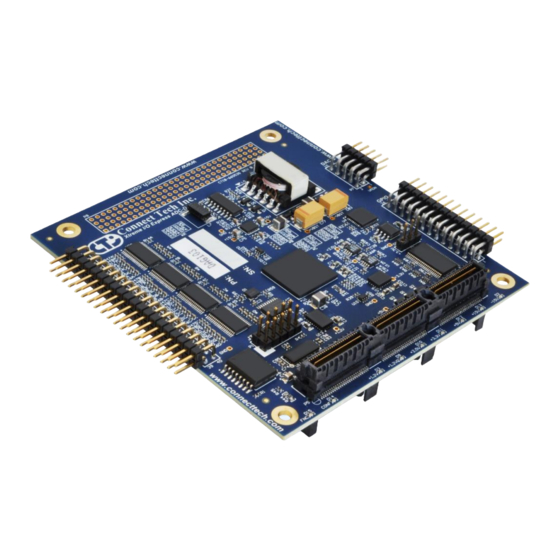
Xtreme I/O Express ADC-DAC
Connect Tech Inc.
42 Arrow Road
Guelph, Ontario
N1K 1S6
www.connecttech.com
CTIM-00435 Revision 0.08 2016-11-18
Connect Tech Xtreme I/O Express ADC-DAC User Manual
Tel:
519-836-1291
Toll:
800-426-8979 (North America only)
Fax:
519-836-4878
Email:
sales@connecttech.com
support@connecttech.com
Advertisement
Table of Contents

Subscribe to Our Youtube Channel
Summary of Contents for Connect Tech Xtreme I/O Express ADC-DAC
- Page 1 Connect Tech Xtreme I/O Express ADC-DAC User Manual Xtreme I/O Express ADC-DAC Connect Tech Inc. Tel: 519-836-1291 42 Arrow Road Toll: 800-426-8979 (North America only) Guelph, Ontario Fax: 519-836-4878 N1K 1S6 Email: sales@connecttech.com www.connecttech.com support@connecttech.com CTIM-00435 Revision 0.08 2016-11-18...
-
Page 2: Preface
The information contained within this user’s guide, including but not limited to any product specification, is subject to change without notice. Connect Tech assumes no liability for any damages incurred directly or indirectly from any technical or typographical errors or omissions contained herein or for discrepancies between the product and the user’s guide. -
Page 3: Limited Product Warranty
Connect Tech Inc. provides a 2 year Warranty for this product. Should this product, in Connect Tech Inc.'s opinion, fail to be in good working order during the warranty period, Connect Tech Inc. will, at its option, repair or replace this product at no charge, provided that the product has not been subjected to abuse, misuse, accident, disaster or non-Connect Tech Inc. -
Page 4: Copyright Notice
Copyright Notice The information contained in this document is subject to change without notice. Connect Tech Inc. shall not be liable for errors contained herein or for incidental consequential damages in connection with the furnishing, performance, or use of this material. This document contains proprietary information that is protected by copyright. -
Page 5: Revision History
Updated overall manual format and organization Revised information on PWM controller, interrupt controller, common board features Add C code examples, and header file 0.08 2016-11-18 Minor updates Document: CTIM-00435 Page 5 of 47 Date: 2016-11-18 Revision: 0.08 Connect Tech Inc. 800-426-8979 | 519-836-1291... -
Page 6: Table Of Contents
CH0_DATA / CH1_DATA (Offset 0x0004 : Read/Write) ................24 CH2_DATA / CH3_DATA (Offset 0x0008 : Read/Write) ................25 CH0_ZERO / CH0_GAIN (Offset 0x000C : Read/Write) ................25 Document: CTIM-00435 Page 6 of 47 Date: 2016-11-18 Revision: 0.08 Connect Tech Inc. 800-426-8979 | 519-836-1291... - Page 7 Example A – writing/reading from scratch pad ................... 41 Example B – reading ID registers ......................... 42 PCIE-104 Interface ............................. 43 Typical Installation ........................... 45 Appendix – A Header File ........................ 46 Document: CTIM-00435 Page 7 of 47 Date: 2016-11-18 Revision: 0.08 Connect Tech Inc. 800-426-8979 | 519-836-1291...
-
Page 8: Introduction
Users Guide www.connecttech.com Introduction Connect Tech’s Xtreme I/O Express ADC-DAC is an analog and digital peripheral board for the PCI- 104 small form factor embedded marketplace. This product is ideal for data acquisition, measurement and control applications. Product Features & Specifications... - Page 9 Humiseal 1B31 Conformal Coating To order any of these part numbers or to inquire about the other available ordering options please contact sales@connecttech.com for further information. Document: CTIM-00435 Page 9 of 47 Date: 2016-11-18 Revision: 0.08 Connect Tech Inc. 800-426-8979 | 519-836-1291...
-
Page 10: Product Overview
Product Overview The Xtreme I/O Express ADC-DAC is based on a custom FPGA controller, SPI ADCs and DAC’s. The following block diagram shows the connection between the interfaces. Each SPI bus is independent, and managed by separate control block. Connection to analog signals are provided by two standard connectors. -
Page 11: Connector Summary & Locations
General Purpose Inputs and Outputs Analog Inputs JTAG programming Analog Outputs PCI-104 Connector Jumper Summary & Locations Designator Description General Purpose Input and Output Voltage Level Document: CTIM-00435 Page 11 of 47 Date: 2016-11-18 Revision: 0.08 Connect Tech Inc. 800-426-8979 | 519-836-1291... -
Page 12: Detailed Feature Description
The following sections describe the operation of each controller, list the pinouts of associated connectors and jumpers, provide memory map, list of registers, and software examples using Connect Tech’s UFD (universal FPGA Driver). Document: CTIM-00435 Page 12 of 47 Date: 2016-11-18 Revision: 0.08 Connect Tech Inc. 800-426-8979 | 519-836-1291... -
Page 13: Analog Inputs (Adc's)
Analog Inputs (ADC’s) Overview The Xtreme I/O Express ADC-DAC uses four Texas Instruments ADS8688, each having an 8-channel multiplexer that allows for the sampling of 8 single ended analog signals. The SPI interface of each ADS8688 is connected to the FPGA controller, while the analog side is connected to right angle header connector. -
Page 14: Operation
ADC peripherals. If slower sampling rates are required, then each block can be individually set to subdivide this maximum rate by way of a counter roll over value stored in the CLK_DIV_CNTR register. Document: CTIM-00435 Page 14 of 47 Date: 2016-11-18 Revision: 0.08 Connect Tech Inc. 800-426-8979 | 519-836-1291... -
Page 15: Memory Map
CH2-LAST_SAMPLE 0x001C CH5-LAST_SAMPLE CH4-LAST_SAMPLE 0x0020 CH7-LAST_SAMPLE CH6-LAST_SAMPLE 0x0024 MEM_WRITE_CONTROL 0x1000 CHANNEL_ID/TIMESTAMP_0 MEM_SAMPLE_0 0x1004 CHANNEL_ID/TIMESTAMP_1 MEM_SAMPLE_1 0x1008 CHANNEL_ID/TIMESTAMP_2 MEM_SAMPLE_2 … … … 0x2FFC CHANNEL_ID/TIMESTAMP_4k MEM_SAMPLE_2k Document: CTIM-00435 Page 15 of 47 Date: 2016-11-18 Revision: 0.08 Connect Tech Inc. 800-426-8979 | 519-836-1291... -
Page 16: Register Details
(NFS) input voltage. The LSB size is equal to FSR / 65536 because the resolution of the ADC is 16 bits. Document: CTIM-00435 Page 16 of 47 Date: 2016-11-18 Revision: 0.08 Connect Tech Inc. 800-426-8979 | 519-836-1291... - Page 17 0x8000 20.48V 0.00V 0xffff 20.48V 10.24V 0x0000 10.24V -5.12V 0x8000 10.24V 0.00V 0xffff 10.24V 5.12V 0x0000 5.12V 0.00V 0x8000 5.12V 2.56V 0xffff 5.12V 5.12V Document: CTIM-00435 Page 17 of 47 Date: 2016-11-18 Revision: 0.08 Connect Tech Inc. 800-426-8979 | 519-836-1291...
-
Page 18: Mem_Write_Control (Adc# Offset 0X0024 : Read/Write(Partial)
0x2046 is the maximum trigger level; in order to prevent counter rollover. Application Examples These application examples leverage the Connect Tech’s Universal FPGA Driver (UFD) and API Example A – ADC Operation with same input range In this example we will set the 2 ADC IC’s to enable sampling, and set the input range for each of the ADCs to be +/-10.24V. -
Page 19: Example B - Adc Operation With Different Input Range
Ch%d, Address %x, CODE=%04x Voltage=%08f\n", i, ADC0+CH0_LAST_SAMPLE+(i*2),testreg, ADC0votlage); i=0; CTIFPGARdWord(pbrd, BarIndex, ADC1+CH0_LAST_SAMPLE+(i*2), &testreg); ADC1votlage = testreg * (20.48/0x10000); printf("ADC1 Ch%d, Address %x, CODE=%04x Voltage=%08f\n", i, ADC1+CH0_LAST_SAMPLE+(i*2),testreg, ADC1votlage); Document: CTIM-00435 Page 19 of 47 Date: 2016-11-18 Revision: 0.08 Connect Tech Inc. 800-426-8979 | 519-836-1291... -
Page 20: Analog Outputs (Dac's)
Users Guide www.connecttech.com Analog Outputs (DAC’s) Overview The Xtreme I/O Express ADC-DAC uses a 16-bit 4-channel DAC IC which is interfaced to the on- http://www.ti.com/lit/gpn/dac8734 board FPGA. The DAC IC datasheet can be found here: Connectors & Jumpers Function Analog Inputs... -
Page 21: Pwm Mode
Since The DAC has settling time of 6 us, the high count and low counr should be at least 4 or 5 times the settling time. Document: CTIM-00435 Page 21 of 47 Date: 2016-11-18 Revision: 0.08 Connect Tech Inc. 800-426-8979 | 519-836-1291... -
Page 22: Transfer Functions
± 0.0488% of full-scale range. The Zero Register uses a twos complement data format in both bipolar and unipolar modes of operation. [DAC8734 Internal] - DACx Gain Code Document: CTIM-00435 Page 22 of 47 Date: 2016-11-18 Revision: 0.08 Connect Tech Inc. 800-426-8979 | 519-836-1291... - Page 23 1 LSB/step, and the total adjustment is typically – 128 LSB to +127 LSB, or ± 0.195% of full-scale range. The Gain Register uses a twos complement data format in both bipolar and unipolar modes of operation. Document: CTIM-00435 Page 23 of 47 Date: 2016-11-18 Revision: 0.08 Connect Tech Inc. 800-426-8979 | 519-836-1291...
-
Page 24: Memory Map
31 30 29 28 27 26 25 24 23 22 21 20 19 18 17 16 15 14 13 12 11 10 9 CH1_DATA CH0_DATA Analog outputs codes for CH0 and CH1 Document: CTIM-00435 Page 24 of 47 Date: 2016-11-18 Revision: 0.08 Connect Tech Inc. 800-426-8979 | 519-836-1291... -
Page 25: Ch2_Data / Ch3_Data (Offset 0X0008 : Read/Write)
CH1_ZERO CH1_GAIN CH1_ZERO stores user-calibration data that is used to eliminate offset error CH1_GAIN stores user-calibration data that is used to eliminate gain error Document: CTIM-00435 Page 25 of 47 Date: 2016-11-18 Revision: 0.08 Connect Tech Inc. 800-426-8979 | 519-836-1291... -
Page 26: Ch2_Zero / Ch2_Gain (Offset 0X0014 : Read/Write)
This register communicates directly with the SPI connected DAC IC. Whatever data is in this register gets shifted out to the DAC IC. This allows access to the DAC IC’s internal register bank which is detailed below: Document: CTIM-00435 Page 26 of 47 Date: 2016-11-18 Revision: 0.08 Connect Tech Inc. 800-426-8979 | 519-836-1291... - Page 27 DAC0 ZERO CODE DAC1 ZERO CODE DAC2 ZERO CODE DAC3 ZERO CODE DAC0 GAIN CODE DAC1 GAIN CODE DAC2 GAIN CODE DAC3 GAIN CODE Document: CTIM-00435 Page 27 of 47 Date: 2016-11-18 Revision: 0.08 Connect Tech Inc. 800-426-8979 | 519-836-1291...
-
Page 28: Trg_Siggen_Pwm (Offset 0X0024 : Read/Write)
31 30 29 28 27 26 25 24 23 22 21 20 19 18 17 16 15 14 13 12 11 10 9 Reserved / Future Use CHAN PWM Frequency Factor Document: CTIM-00435 Page 28 of 47 Date: 2016-11-18 Revision: 0.08 Connect Tech Inc. 800-426-8979 | 519-836-1291... -
Page 29: Pwm_High_Val / Pwm_Low_Val (Offset 0X0034 : Read/Write)
The DAC code to output when the PWM signal is output as high PWM_LOW_VAL The DAC code to output when the PWM signal is output as low Document: CTIM-00435 Page 29 of 47 Date: 2016-11-18 Revision: 0.08 Connect Tech Inc. 800-426-8979 | 519-836-1291... -
Page 30: Application Examples
CTIFPGAWrDword(pbrd, BarIndex, DAC0 + PWM_LOW_VAL, pwmLvl); // Enabling pulse gen pwmCtrl = (0x0 << 16) | (freqMult << 8) | 0x8 | 0x4; CTIFPGAWrDword(pbrd, BarIndex, DAC0 + PWM_CTRL, pwmCtrl); Document: CTIM-00435 Page 30 of 47 Date: 2016-11-18 Revision: 0.08 Connect Tech Inc. 800-426-8979 | 519-836-1291... - Page 31 Xtreme I/O Express ADC-DAC Users Guide www.connecttech.com siggen = 0x3; CTIFPGAWrDword(pbrd, BarIndex, DAC0 + TRG_SIGGEN_PWM, siggen); return; Document: CTIM-00435 Page 31 of 47 Date: 2016-11-18 Revision: 0.08 Connect Tech Inc. 800-426-8979 | 519-836-1291...
-
Page 32: Example C: Sine Wave Generation
CTIFPGAWrDword(pbrd, BarIndex, DAC0 + CH2_DATA, 0x0); for(i=0; i<DAC_MEM_DWORDS; i++) wrCode = (dacCode[2*i+1] << 16) | (0xFFFF & dacCode[2*i]); addr = DAC0 + SIG_GEN_MEM_0 + i*4; CTIFPGAWrDword(pbrd, BarIndex, addr, wrCode); Document: CTIM-00435 Page 32 of 47 Date: 2016-11-18 Revision: 0.08 Connect Tech Inc. 800-426-8979 | 519-836-1291... - Page 33 CTIFPGAWrDword(pbrd, BarIndex, DAC0 + SIG_GEN_RD_CTRL, ctrl); divcntr = 2; CTIFPGAWrDword(pbrd, BarIndex, DAC0 + SAMPLE_DIV_CNTR, divcntr); // enable the signal genarator siggen = 0x2; CTIFPGAWrDword(pbrd, BarIndex, DAC0 + TRG_SIGGEN_PWM, siggen); Document: CTIM-00435 Page 33 of 47 Date: 2016-11-18 Revision: 0.08 Connect Tech Inc. 800-426-8979 | 519-836-1291...
-
Page 34: Gpio (Digital I/O)
GPIO (Digital I/O) Overview The Xtreme I/O Express ADC-DAC has 16-bits of bi-directional GPIO that can be configured to operate with +3.3V or +5V logic levels. The upper and lower 8 bytes (GPIO0–GPIO7 = lower | GPIO8-GPIO15=upper) can be set to either inputs or outputs independently. -
Page 35: Operation
GPIO0 and bit-9 = GPIO9. Reading a ‘1’ from the bit location means that the state of the input pin is logic HIGH, reading ‘0’ means the state of the input pin is logic LOW. Document: CTIM-00435 Page 35 of 47 Date: 2016-11-18 Revision: 0.08 Connect Tech Inc. 800-426-8979 | 519-836-1291... -
Page 36: Gpio_Output (Offset 0X0004 : Read/Write)
= FALSE; else printf("OK!\n"); // Shift the 1 over outgpio = outgpio << 1; // Walking 0 test outgpio = 0xFE; printf("Walking 0's\n"); Document: CTIM-00435 Page 36 of 47 Date: 2016-11-18 Revision: 0.08 Connect Tech Inc. 800-426-8979 | 519-836-1291... - Page 37 // Compare Values (outgpio != ingpio){ printf("ERROR MIS-MATCH\n"); result = FALSE; else printf("OK!\n"); // Shift the 0 over outgpio = (outgpio <<1) + 1; Document: CTIM-00435 Page 37 of 47 Date: 2016-11-18 Revision: 0.08 Connect Tech Inc. 800-426-8979 | 519-836-1291...
-
Page 38: Flash Controller
0x0008 SPI_STATUS 0x000C SPI_RESULT 0x00100 SPI_PAGE_MEM Register Details For futher details on the flash controller operation, contact support@connecttech.com to obtain the necessary software package. Document: CTIM-00435 Page 38 of 47 Date: 2016-11-18 Revision: 0.08 Connect Tech Inc. 800-426-8979 | 519-836-1291... -
Page 39: Common Features
31 30 29 28 27 26 25 24 23 22 21 20 19 18 17 16 15 14 13 12 11 10 9 8 7 6 5 4 3 2 1 0 Document: CTIM-00435 Page 39 of 47 Date: 2016-11-18 Revision: 0.08 Connect Tech Inc. 800-426-8979 | 519-836-1291... -
Page 40: Irq_Mstr_Status (Irq_Base +0X40 : Read Only)
DAC controller block has a pending interrupt FLASH SPI Flash controller block has a pending interrupt This is the overall interrupt status for each functional block. Document: CTIM-00435 Page 40 of 47 Date: 2016-11-18 Revision: 0.08 Connect Tech Inc. 800-426-8979 | 519-836-1291... -
Page 41: Irq_Mstr_Enable (Irq_Base +0X50 : Read/Write Only)
= CTIFPGARdDword(pbrd, BAR_MAIN, COMMON_BASE+SCRATCHPAD_REG_1, &rdreg); if(ret != CTI_STATUS_OK) printf("Error read from FPGA mem"); result = FALSE; else printf ("rd reg = 0x%08x \n", rdreg); Document: CTIM-00435 Page 41 of 47 Date: 2016-11-18 Revision: 0.08 Connect Tech Inc. 800-426-8979 | 519-836-1291... -
Page 42: Example B - Reading Id Registers
FPGA mem"); result = FALSE; else rawtime = tsreg; timeinfo = localtime(&rawtime); printf ("Timestamp reg = 0x%08x , %s\n", idreg, asctime(timeinfo)); Document: CTIM-00435 Page 42 of 47 Date: 2016-11-18 Revision: 0.08 Connect Tech Inc. 800-426-8979 | 519-836-1291... -
Page 43: Pcie-104 Interface
PCIE-104 Interface The below table details the pinout of the PCIe/104 connector and what pins/signals are used on the Xtreme I/O Express ADC-DAC. Note this product only uses the +5V rail power connection and a single x1 PCI Express Link. - Page 44 NC/Pass-Thru NC/Pass-Thru NC/Pass-Thru NC/Pass-Thru NC/Pass-Thru NC/Pass-Thru NC/Pass-Thru NC/Pass-Thru NC/Pass-Thru NC/Pass-Thru NC/Pass-Thru NC/Pass-Thru NC/Pass-Thru NC/Pass-Thru NC/Pass-Thru NC/Pass-Thru NC/Pass-Thru NC/Pass-Thru NC/Pass-Thru NC/Pass-Thru NC/Pass-Thru NC/Pass-Thru NC/Pass-Thru NC/Pass-Thru Document: CTIM-00435 Page 44 of 47 Date: 2016-11-18 Revision: 0.08 Connect Tech Inc. 800-426-8979 | 519-836-1291...
-
Page 45: Typical Installation
Typical Installation 1) Ensure the target system is powered off. 2) Insert the Xtreme I/O Express ADC-DAC onto PCI-104 Express stack; clip into place depending on the available mounting hardware. 3) Attached the application cabling to the analog input connector , analog output connector, and GPIO connector. -
Page 46: Appendix - A Header File
#define CH3_GAIN 0x18 #define CH3_ZERO 0x19 #define IO_PINS_CONTROL 0x1C #define CMD_PASSTHRU 0x20 #define TRG_SIGGEN_PWM 0x24 #define SIG_GEN_RD_CTRL 0x28 #define PWM_LOW_COUNT 0x2C #define PWM_HIGH_COUNT 0x2E Document: CTIM-00435 Page 46 of 47 Date: 2016-11-18 Revision: 0.08 Connect Tech Inc. 800-426-8979 | 519-836-1291... - Page 47 FLASH_BASE 0x24000 #define SPI_CMD 0x0000 #define SPI_PARAM 0x0004 #define SPI_STATUS 0x0008 #define SPI_RESULT 0x000C #define SPI_PAGE_MEM 0x0100 #define ID_BASE 0x24210 #define RELEASE #define TIMESTAMP Document: CTIM-00435 Page 47 of 47 Date: 2016-11-18 Revision: 0.08 Connect Tech Inc. 800-426-8979 | 519-836-1291...
Need help?
Do you have a question about the Xtreme I/O Express ADC-DAC and is the answer not in the manual?
Questions and answers