Advertisement
Quick Links
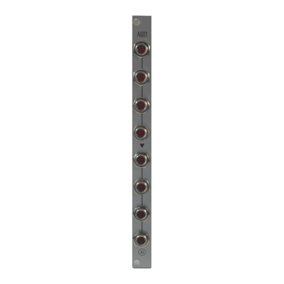
AI Synthesis AI001 Multiple:
This is the Build Guide for the
http://aisynthesis.com/product/eurorackmultiplediykit/.
Table of Contents:
1. Resources
2. About the Multiple
3. Tools Needed
4. BOM
5. Build Steps
1. Resources
1. Schematic
Build Guide
A I001 Multiple
, you can purchase it by going to:
Advertisement

Summary of Contents for AI Synthesis AI001 Multiple
- Page 1 AI Synthesis AI001 Multiple: Build Guide This is the Build Guide for the A I001 Multiple , you can purchase it by going to: http://aisynthesis.com/product/eurorackmultiplediykit/. Table of Contents: 1. Resources 2. About the Multiple 3. Tools Needed 4. BOM 5. Build Steps 1. Resources 1. Schematic ...
- Page 2 2. About the Multiple It is critically important to be able to split and distribute your modular’s signals to multiple destinations, and the A I001 Multiple module does just that. Because the module takes up only 2HP, it can be placed anywhere. The multiple can be used as either a 2×4 passive multiple, or as a 1×7. The first set of four are linked together, and if nothing is plugged into the 5th jack, then that signal continues on to the 6th, 7th, and 8th jack as well. If a cable is plugged into the 5th jack, then that signal is distributed to the 6th, 7th, and 8th jacks and it functions as a 2×4 multiple. That’s confusing. Let’s look at the jacks, and then the schematic: ...
- Page 3 Each jack has three lugs: 1 is the ground, 3 is the signal, and 2 is a switch. When no jack is inserted, pin 2 is connected (or “normalled” to pin 3. ...
- Page 4 ...
- Page 5 In our Multiple, only In2 uses this switched jack. When no jack is inserted into In2, signal passes from In1, O1, O2, and O3 onto O4, O5, and O6. Inserting a jack into In2 breaks this switch, and so the signal from In2 passes to O4, O5, and O6. We say this unit is passive, because it requires no power to operate. Because the multiple is passive, each time a signal is “tapped,” it will be slightly weaker. In the case of distributing gate, audio, or control voltage signals where v/octave control is not needed, the effect should be fairly negligible. In the use case of distributing pitch voltage (to multiple oscillators) a different “buffered” multiple module should be used. A buffered multiple requires power and uses Operational amplifiers to distribute voltage without any signal drop. Nonetheless, this passive multiple is an indispensable module, and its thin space means it can be easily included next to envelopes, clocks, gate generators, and other modules that benefit from voltage distribution. 3. Tools Needed ● Soldering Iron ( C heap or N ice ) ● Solder ● Soldering Tip Cleaner ...
- Page 6 4. BOM In the kit: 2 Mounting Screws, a PCB, an aluminum panel, 8 jacks, 8 nuts, a card linking to these instructions, and a sticker. Because this is a passive module, no power cable is included. Category Part Quantity Hardware 3.5mm Thonkiconn Jack 8 Hardware Jack Nuts 8 Hardware Panel 1 ...
- Page 7 Hardware PCB 1 5. Build Steps There is a full build guide video here: ttps://youtu.be/mkWVKhYoU8k 1. Gather the panel, tools, pcb, and jacks. 2. Place the jacks into the holes as shown above. 3. Solder the Jacks – To view a video example, go to: h ttps://youtu.be/qJHCtUuXRHg . Soldering is the heart and soul of DIY electronics, and it’s why I suggest getting a nice soldering iron. Only use enough solder to get the job done. Most soldering problems arise by using too much solder. It is easy to get carried away or frustrated and glob a blob of solder on the connection. For this kit, I have my iron at 550 degrees Fahrenheit (287 Celcius). Heat the connection for about half a second before you apply solder. This preheating will prevent the molten solder from hitting cold metal and cooling too fast. This results in what’s called a ‘cold solder joint’, which is a loose connection where the solder did not adhere to the metal. ...
- Page 8 These can be very frustrating, as at a casual glance will they will often appear to be good connections, and only upon close examination will one see the cracks, The technique (which becomes automatic after a while) is to put the tip on the connection first, and then apply the solder. Once the solder is on the joint, you hold the iron there for another half second, and pull the iron away. If the solder doesn’t flow easily, perhaps you haven’t allowed your iron to warm up, or you need to clean your iron tip. I like a temperature of about 550 degrees Fahrenheit for leaded solder. 4. Place the panel onto the PCB with the jacks. The Jack labeled “In1” on the PCB goes in the top hole of the panel, below AI001. Now carefully tighten the nuts. 5. Testing: Begin by testing the first configuration. See the image above. In the first configuration, the red cable is feeding in a signal, and each yellow cable is distributing that signal elsewhere.This is easily tested by using an oscillator or mp3 player, and listening to the other jacks via headphones. The fifth jack is not used, as that is a switched jack. When a ...
- Page 9 plug is inserted into the fifth jack the multiple changes from a 1×7 to a 2×4 multiple. 6. The image above shows a 2×4 configuration, The red cable is feeding signal in, and the signal is being distributed via the three yellow cables elsewhere. The blue cable is feeding a separate signal in, and distributing it elsewhere via the three white cables. This is easily tested by using an oscillator or mp3 player, and listening to the other jacks via headphones. 7. If things are not working, use a multimeter on continuity mode and test for continuity in accordance with the schematic (all grounds should have connectivity, and with no cables inserted, there should be continuity between all signal lugs, jack 5’s switched jack should have continuity with input 1’s signal jack). The three most likely errors are: 1) There is a cold solder joint. Inspect closely looking for a poor solder joint, and reflow solder if necessary. 2) A jack is somehow inserted incorrectly. There is only one way for all jacks to fit this PCB, so this would be hard to do, but it is possible. Finally, ensure that you soldered the jacks to the correct side of the board by comparing your build with the pictures in this guide. 8. Share your build on F acebook at: https://www.facebook.com/AISynthesis1123432724366073/?fref=ts ! 9. If you are having any issues at all, please c ontact us at: http://aisynthesis.com/contact/. ...
Need help?
Do you have a question about the AI001 Multiple and is the answer not in the manual?
Questions and answers