
Related Manuals for National Instruments AT-MIO-64F-5


Summary of Contents for National Instruments AT-MIO-64F-5
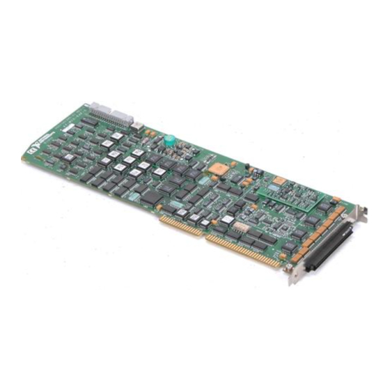
- Page 1 AT-MIO-64F-5 User Manual Multifunction I/O Board for the PC AT/EISA July 1994 Edition Part Number 320487-01 © Copyright 1992, 1994 National Instruments Corporation. All Rights Reserved.
- Page 2 National Instruments Corporate Headquarters 6504 Bridge Point Parkway Austin, TX 78730-5039 (512) 794-0100 Technical support fax: (800) 328-2203 (512) 794-5678 Branch Offices: Australia (03) 879 9422, Austria (0662) 435986, Belgium 02/757.00.20, Canada (Ontario) (519) 622-9310, Canada (QuŽbec) (514) 694-8521, Denmark 45 76 26 00, Finland (90) 527 2321, France (1) 48 14 24 24, Germany 089/741 31 30, Italy 02/48301892, Japan (03) 3788-1921, Netherlands 03480-33466, Norway 32-848400, Spain (91) 640 0085, Sweden 08-730 49 70, Switzerland 056/27 00 20, U.K.
- Page 3 Any action against National Instruments must be brought within one year after the cause of action accrues. National Instruments shall not be liable for any delay in performance due to causes beyond its reasonable control. The warranty provided herein does not cover damages, defects, malfunctions, or service failures caused by owner's failure to follow the National Instruments installation, operation, or maintenance instructions;...
- Page 4 Any use or application of National Instruments products for or involving medical or clinical treatment must be performed by properly trained and qualified medical personnel, and all traditional medical safeguards, equipment, and procedures that are appropriate in the particular situation to prevent serious injury or death should always continue to be used when National Instruments products are being used.
- Page 5 Preface This manual describes the mechanical and electrical aspects of the AT-MIO-64F-5 board and contains information concerning its operation and programming. The AT-MIO-64F-5 is a high- performance, multifunction analog, digital, and timing I/O board for the IBM PC AT and compatible computers and EISA personal computers (PCs).
- Page 6 The following abbreviations are used in this manual: amperes decibels feet farads hexadecimal hertz ksamples 1,000 samples megabytes of memory meters ohms percent parts per million root mean square seconds volts Vref reference voltage Vrms volts, root mean square AT-MIO-64F-5 User Manual © National Instruments Corporation...
- Page 7 ¥ IBM Personal Computer AT Technical Reference manual You may also want to consult the following Advanced Micro Devices manual if you plan to program the Am9513A Counter/Timer used on the AT-MIO-64F-5: ¥ Am9513A/Am9513 System Timing Controller technical manual For more information on the effects of dither, see the following article: ¥...
- Page 8 Preface Customer Communication National Instruments wants to receive your comments on our products and manuals. We are interested in the applications you develop with our products, and we want to help if you have problems with them. To make it easy for you to contact us, this manual contains comment and configuration forms for you to complete.
-
Page 9: Table Of Contents
Differential Connection Considerations (DIFF Input Configuration) ...2-21 Differential Connections for Ground-Referenced Signal Sources..2-22 Differential Connections for Nonreferenced or Floating Signal Sources....................2-23 Single-Ended Connection Considerations ..........2-24 Single-Ended Connections for Floating Signal Sources (RSE Configuration)..................2-25 © National Instruments Corporation AT-MIO-64F-5 User Manual... - Page 10 FIFO Programmed Cyclic Waveform Generation.........3-18 FIFO Pulsed Waveform Generation ............3-18 Digital I/O Circuitry.......................3-19 Timing I/O Circuitry ......................3-20 RTSI Bus Interface Circuitry ..................3-23 Chapter 4 Register Map and Descriptions ..................4-1 Register Map........................4-1 Register Sizes.....................4-2 AT-MIO-64F-5 User Manual © National Instruments Corporation...
- Page 11 Chapter 5 Programming ........................5-1 Register Programming Considerations ................5-1 Resource Allocation Considerations................5-1 Initializing the AT-MIO-64F-5..................5-2 Initializing the Am9513A ..................5-2 Programming the Analog Input Circuitry ..............5-4 Single Conversions Using the SCONVERT or EXTCONV* Signal ....5-4 © National Instruments Corporation AT-MIO-64F-5 User Manual...
- Page 12 Calibration Procedures .....................6-1 Calibration Equipment Requirements................6-5 Calibration DACs......................6-5 Calibration Channels......................6-6 Reference Calibration ....................6-6 Analog Input Calibration ....................6-6 Analog Output Calibration.....................6-7 Appendix A Specifications ........................A-1 Analog Input ........................A-1 Explanation of Analog Input Specifications ............A-2 AT-MIO-64F-5 User Manual © National Instruments Corporation...
- Page 14 Contents Figures Figure 1-1. AT-MIO-64F-5 Board..................1-2 Figure 2-1. AT-MIO-64F-5 Parts Locator Diagram.............2-2 Figure 2-2. Example Base I/O Address Switch Settings ............2-3 Figure 2-3. AT-MIO-64F-5 I/O Connector ................2-12 Figure 2-4. 50-Pin MIO Subconnector .................2-13 Figure 2-5. Extended Analog Input Subconnector ...............2-17 Figure 2-6.
- Page 15 Extended Analog Input Subconnector ...............D-1 Tables Table 1-1. Optional Equipment ...................1-4 Table 2-1. Default Settings of National Instruments Products for the PC ......2-4 Table 2-2. Switch Settings with Corresponding Base I/O Address and Base I/O Address Space....................2-5 Table 2-3. Available Input Configurations for the AT-MIO-64F-5........2-6 Table 2-4.
-
Page 17: Chapter 1 Introduction
The AT-MIO-64F-5 is a high-performance multifunction analog, digital, and timing I/O board for the PC. The AT-MIO-64F-5 has a 5 µsec, 12-bit sampling ADC that can monitor a single input channel, or scan through the 64 single-ended or 32 differential channels (expandable with National Instruments multiplexing products) at a programmable gain of 0.5, 1, 2, 5, 10, 20, 50, or... -
Page 18: Digital And Timing I/O
In addition to the analog input and analog output capabilities of the AT-MIO-64F-5, the AT-MIO-64F-5 also has eight digital I/O lines that can sink up to 24 mA of current, and three independent 16-bit counter/timers for frequency counting, event counting, and pulse output applications. -
Page 19: What Your Kit Should Contain
Chapter 1 Introduction What Your Kit Should Contain The contents of the AT-MIO-64F-5 kit (part number 776655-01) are listed as follows. Kit Component Part Number AT-MIO-64F-5 board 181395-01 AT-MIO-64F-5 User Manual 320487-01 NI-DAQ software for DOS/Windows/LabWindows, with manuals 776250-01 NI-DAQ Software Reference Manual for DOS/Windows/LabWindows... -
Page 20: Optional Equipment
0.5-m ribbon cable 776366-05 with 1.0-m ribbon cable 776366-10 with 2.0-m ribbon cable 776366-20 AT Series RTSI bus cables for 2 boards 776249-02 3 boards 776249-03 4 boards 776249-04 5 boards 776249-05 (continues) AT-MIO-64F-5 User Manual © National Instruments Corporation... -
Page 21: Custom Cables
SSR Series mounting rack and 1.0 m cable 8-channel with SC-205X cable Custom Cables The AT-MIO-64F-5 I/O connector is a 100-pin male ribbon-cable header. The manufacturer part number for this header is as follows: ¥ Robinson Nugent (part number P50E-100P1-SR1-TG) The mating connector for the AT-MIO-64F-5 is a 100-position polarized ribbon socket connector. -
Page 22: Unpacking
T&B Ansley Corporation (part number 609-0005) Unpacking Your AT-MIO-64F-5 board is shipped in an antistatic package to prevent electrostatic damage to the board. Several components on the board can be damaged by electrostatic discharge. To avoid such damage in handling the board, take the following precautions: ¥... -
Page 23: Configuration And Installation
AT-MIO-64F-5, and cable considerations. Board Configuration The AT-MIO-64F-5 contains one DIP switch to configure the base address selection for the AT bus interface. The remaining resource selections, such as DMA and interrupt channel selections, are determined by programming the individual registers in the AT-MIO-64F-5 register set. The... -
Page 24: Figure 2-1. At-Mio-64F-5 Parts Locator Diagram
Configuration and Installation Chapter 2 This art not available in PDF version of this document. Figure 2-1. AT-MIO-64F-5 Parts Locator Diagram AT-MIO-64F-5 User Manual © National Instruments Corporation... -
Page 25: At Bus Interface
Base I/O Address Selection The AT-MIO-64F-5 is configured at the factory to a base I/O address of 220 hex. This base address setting is suitable for most systems. However, if your system has other hardware at this base I/O address, you must change either the AT-MIO-64F-5 base address DIP switch or the other hardware base address to avoid a conflict. -
Page 26: Table 2-1. Default Settings Of National Instruments Products For The Pc
(LSBs) of the address (A4 through A0) used by the AT-MIO-64F-5 circuitry to decode the individual register selections. The don't care bits indicate the size of the register space. In this case, the AT-MIO-64F-5 uses I/O address hex 220 through hex 23F in the factory-default setting. -
Page 27: Interrupt And Dma Channel Selection
3E0 - 3FF Interrupt and DMA Channel Selection The base I/O address selection is the only resource on the AT-MIO-64F-5 board that must be set manually before the board is placed into the PC. The interrupt level and DMA channels used by the AT-MIO-64F-5 are selected via registers in the AT-MIO-64F-5 register set. -
Page 28: Analog Input Configuration
Configuration and Installation Chapter 2 The AT-MIO-64F-5 does not use and cannot be configured to use the 8-bit DMA channels 0 through 3 on the PC I/O channel for 16-bit transfers. Analog Input Configuration The analog input section of the AT-MIO-64F-5 is software configurable. You can select different analog input configurations by programming the appropriate register in the AT-MIO-64F-5 register set. -
Page 29: Rse Input (64 Channels)
RSE input means that all input signals are referenced to a common ground point that is also tied to the analog input ground of the AT-MIO-64F-5 board. The negative (-) input of the differential input amplifier is tied to the analog ground. This configuration is useful when measuring floating signal sources. -
Page 30: Input Polarity And Input Range
AT-MIO-64F-5 ADC can accommodate. The AT-MIO-64F-5 board has gains of 0.5, 1, 2, 5, 10, 20, 50, and 100 and is suited for a wide variety of signal levels. With the proper gain setting, the full resolution of the ADC can be used to measure the input signal. -
Page 31: Analog Output Configuration
Analog Output Reference Selection Each DAC can be connected to the AT-MIO-64F-5 internal reference of 10 V or to the external reference signal connected to the EXTREF pin on the I/O connector. This signal applied to EXTREF must be between -10 and +10 V. Both channels need not be configured for the same mode. -
Page 32: Digital I/O Configuration
AT-MIO-64F-5 register set. The AT-MIO-64F-5 can use either its internal 10 MHz timebase, or it can use a timebase received over the RTSI bus. In addition, if the board is configured to use the internal timebase, it can also be programmed to drive its internal timebase over the RTSI bus to another board that is programmed to receive this timebase signal. -
Page 33: Signal Connections
3. Remove the expansion slot cover on the back panel of the computer. 4. Insert the AT-MIO-64F-5 into a 16-bit slot. Do not force the board into place. Verify that there are no extended components on the circuit board of the computer that may touch or be in the way of any part of the AT-MIO-64F-5. - Page 34 ACH59 OUT1 ACH36 EXTTMRTRIG* ACH60 GATE2 ACH37 OUT2 ACH61 SOURCE5 ACH38 GATE5 ACH62 OUT5 ACH39 FOUT ACH63 MIO Subconnector Extended Analog Input Pins Subconnector Pins Figure 2-3. AT-MIO-64F-5 I/O Connector Pin Assignment AT-MIO-64F-5 User Manual 2-12 © National Instruments Corporation...
- Page 35 BDIO2 ADIO2 ADIO3 BDIO3 +5 V DIG GND SCANCLK +5 V EXTSTROBE* EXTTRIG* EXTGATE* EXTCONV* GATE1 SOURCE1 OUT1 EXTTMRTRIG* OUT2 GATE2 SOURCE5 GATE5 OUT5 FOUT Figure 2-4. 50-Pin MIO Subconnector Pin Assignment © National Instruments Corporation 2-13 AT-MIO-64F-5 User Manual...
-
Page 36: Mio Subconnector Signal Connection Descriptions
Digital Ground Ð This pin supplies the reference for the digital signals at the I/O connector as well as the +5 VDC supply. 25, 27, 29, 31 ADIO<0..3> DIG GND Digital I/O port A signals. AT-MIO-64F-5 User Manual 2-14 © National Instruments Corporation... - Page 37 Am9513A Counter 1 signal. GATE1 DIG GND GATE1 Ð This pin is from the Am9513A Counter 1 signal. OUT1 DIG GND OUTPUT1 Ð This pin is from the Am9513A Counter 1 signal. © National Instruments Corporation 2-15 AT-MIO-64F-5 User Manual...
- Page 38 GATE5 Ð This pin is from the Am9513A Counter 5 signal. OUT5 DIG GND OUT5 Ð This pin is from the Am9513A Counter 5 signal. FOUT DIG GND Frequency Output Ð This pin is from the Am9513A FOUT signal. AT-MIO-64F-5 User Manual 2-16 © National Instruments Corporation...
- Page 39 ACH52 ACH28 ACH53 ACH29 ACH30 ACH54 ACH31 ACH55 ACH56 ACH32 ACH33 ACH57 ACH58 ACH34 ACH59 ACH35 ACH36 ACH60 ACH37 ACH61 ACH38 ACH62 ACH39 ACH63 Figure 2-5. Extended Analog Input Subconnector Pin Assignment © National Instruments Corporation 2-17 AT-MIO-64F-5 User Manual...
-
Page 40: Extended Analog Input Subconnector Signal Descriptions
AI GND signal pins. AI GND is an analog input common signal that is routed directly to the ground tie point on the AT-MIO-64F-5. These pins can be used for a general analog power ground tie point to the AT-MIO-64F-5 if necessary. -
Page 41: Figure 2-6. At-Mio-64F-5 Pgia
64 analog input channels of the AT-MIO-64F-5. In single-ended mode, signals connected to ACH<0..63> are routed to the positive (+) input of the AT-MIO-64F-5 PGIA. In differential mode, signals connected to ACH<0..7> and ACH<16..39>are routed to the positive (+) input of the AT-MIO-64F-5 PGIA, and signals connected to ACH<8..15>... -
Page 42: Types Of Signal Sources
AT-MIO-64F-5 ground. The AT-MIO-64F-5 ADC measures this output voltage when it performs A/D conversions. All signals must be referenced to ground, either at the source device or at the AT-MIO-64F-5. If you have a floating source, the AT-MIO-64F-5 should reference the signal to ground by using the RSE input mode or the DIFF input configuration with bias resistors (see the Differential Connections for Nonreferenced or Floating Signal Sources section later in this chapter). -
Page 43: Differential Connection Considerations (Diff Input Configuration)
DIFF with bias resistors Differential Connection Considerations (DIFF Input Configuration) Differential connections are those in which each AT-MIO-64F-5 analog input signal has its own reference signal or signal return path. These connections are available when the AT-MIO-64F-5 is configured in the DIFF input mode. Each input signal is tied to the positive (+) input of the PGIA, and its reference signal, or return, is tied to the negative (-) input of the PGIA. -
Page 44: Differential Connections For Ground-Referenced Signal Sources
Chapter 2 Differential Connections for Ground-Referenced Signal Sources Figure 2-7 shows how to connect a ground-referenced signal source to an AT-MIO-64F-5 board configured in the DIFF input mode. The AT-MIO-64F-5 analog input circuitry must be configured for DIFF input to make these types of connections. Configuration instructions are included in Chapter 4, Register Map and Descriptions. -
Page 45: Differential Connections For Nonreferenced Or Floating Signal Sources
Configuration and Installation Differential Connections for Nonreferenced or Floating Signal Sources Figure 2-8 shows how to connect a floating signal source to an AT-MIO-64F-5 board configured in the DIFF input mode. The AT-MIO-64F-5 analog input circuitry must be configured for DIFF input to make these types of connections. -
Page 46: Single-Ended Connection Considerations
PGIA, and their common ground point is tied to the negative (-) input of the PGIA. When the AT-MIO-64F-5 is configured for single-ended input, up to 64 analog input channels are available. Single-ended input connections can be used when all input signals meet the following criteria: ¥... -
Page 47: Single-Ended Connections For Floating Signal Sources (Rse Configuration)
AT-MIO-64F-5 provides the reference ground point for the external signal. The NRSE input configuration is used for ground-referenced signal sources; in this case, the external signal supplies its own reference ground point and the AT-MIO-64F-5 should not supply one. -
Page 48: Single-Ended Connections For Grounded Signal Sources (Nrse Configuration)
(+) and negative (-) inputs of the PGIA and this difference is rejected by the amplifier. On the other hand, if the input circuitry of the AT-MIO-64F-5 is referenced to ground, such as in the RSE input configuration, this difference in ground potentials appears as an error in the measured voltage. -
Page 49: Analog Output Signal Connections
Chapter 2 Configuration and Installation The common-mode input range of the AT-MIO-64F-5 PGIA is defined as the magnitude of the greatest common-mode signal that can be rejected. The PGIA can reject common-mode signals as long as V + and V - are both in the range ±12 V. -
Page 50: Digital I/O Signal Connections
2 V minimum input logic low voltage 0.8 V maximum input current load, logic high input voltage 40 µA maximum input current load, logic low input voltage -120 µA maximum AT-MIO-64F-5 User Manual 2-28 © National Instruments Corporation... -
Page 51: Figure 2-12. Digital I/O Connections
Digital input applications include receiving TTL signals and sensing external device states such as the state of the switch in Figure 2-12. Digital output applications include sending TTL signals and driving external devices such as the LED shown in Figure 2-12. © National Instruments Corporation 2-29 AT-MIO-64F-5 User Manual... -
Page 52: Power Connections
Warning: Under no circumstances should these +5-V power pins be directly connected to analog or digital ground or to any other voltage source on the AT-MIO-64F-5 or any other device. Doing so can damage the AT-MIO-64F-5 and the PC. National Instruments is not liable for damages resulting from such a connection. -
Page 53: Figure 2-14. Extconv* Signal Timing
Note: EXTCONV* and the output of Counter 3 of the Am9513A are physically connected together on the AT-MIO-64F-5. If Counter 3 is used in an application, the EXTCONV* signal must be left undriven. Conversely, if EXTCONV* is used in an application, Counter 3 must be disabled. -
Page 54: Figure 2-15. Exttrig* Signal Timing
EXTTMRTRIG* Signal The analog output DACs on the AT-MIO-64F-5 can be updated using either internal or external signals in posted update mode. The DACs can be updated externally by using the EXTTMRTRIG* signal from the I/O connector. This signal updates the DACs when A4RCV is disabled and the appropriate DAC waveform mode is programmed through one of the registers in the AT-MIO-64F-5 register set. -
Page 55: General-Purpose Timing Signal Connections
Counter operation can be gated on and off during event counting. Figure 2-17 shows connections for a typical event-counting operation in which a switch is used to gate the counter on and off. © National Instruments Corporation 2-33 AT-MIO-64F-5 User Manual... -
Page 56: Figure 2-17. Event-Counting Application With External Switch Gating
Figure 2-18 shows the connections for a frequency measurement application. A second counter can also be used to generate the gate signal in this application. AT-MIO-64F-5 User Manual 2-34 © National Instruments Corporation... -
Page 57: Figure 2-18. Frequency Measurement Application
Am9513A digital output specifications (referenced to DIG GND): output logic high voltage 2.4 V minimum output logic low voltage 0.4 V maximum output source current, at V 200 µA maximum output sink current, at V 3.2 mA maximum © National Instruments Corporation 2-35 AT-MIO-64F-5 User Manual... -
Page 58: Figure 2-19. General-Purpose Timing Signals
AT-MIO-64F-5. This clock signal is selected by a register in the AT-MIO-64F-5 register set and then divided by 10. The default value is 1 MHz into the Am9513A (10 MHz clock signal on the AT-MIO-64F-5). The... -
Page 59: Field Wiring Considerations
Use individually shielded, twisted-pair wires to connect analog input signals to the AT-MIO-64F-5. With this type of wire, the signals attached to the CH+ and CH- inputs are twisted together and then covered with a shield. This shield is then connected only at one point to the signal source ground. -
Page 60: Cabling Considerations
Configuration and Installation Chapter 2 ¥ Do not run AT-MIO-64F-5 signal lines through conduits that also contain power lines. ¥ Protect AT-MIO-64F-5 signal lines from magnetic fields caused by electric motors, welding equipment, breakers, or transformers by running the AT-MIO-64F-5 signal lines through special metal conduits. -
Page 61: Chapter 3 Theory Of Operation
Chapter 3 Theory of Operation This chapter contains a functional overview of the AT-MIO-64F-5 and explains the operation of each functional unit making up the AT-MIO-64F-5. Functional Overview The block diagram in Figure 3-1 is a functional overview of the AT-MIO-64F-5 board. -
Page 62: Pc I/O Channel Interface Circuitry
PC I/O Channel Interface Circuitry The AT-MIO-64F-5 board is a full-size 16-bit PC I/O channel adapter. The PC I/O channel consists of a 24-bit address bus, a 16-bit data bus, a DMA arbitration bus, interrupt lines, and several control and support signals. -
Page 63: Figure 3-2. Pc I/O Channel Interface Circuitry Block Diagram
AT-MIO-64F-5 multiple-function circuitry. The PC I/O channel has 24 address lines; the AT-MIO-64F-5 uses 10 of these lines to decode the board address. Therefore, the board address range is 000 to 3FF hex. SA5 through SA9 are used to generate the board enable signal. -
Page 64: Analog Input And Data Acquisition Circuitry
AT-MIO-64F-5ÐIRQ3, IRQ4, IRQ5, IRQ7, IRQ10, IRQ11, IRQ12, and IRQ15. These interrupt levels are selectable from one of the registers in the AT-MIO-64F-5 register set. Six different interrupts can be generated by the AT-MIO-64F-5. Each of the following cases is individually enabled and cleared: ¥... -
Page 65: Figure 3-3. Analog Input And Data Acquisition Circuitry Block Diagram
Chapter 3 Theory of Operation Figure 3-3. Analog Input and Data Acquisition Circuitry Block Diagram © National Instruments Corporation AT-MIO-64F-5 User Manual... -
Page 66: Analog Input Circuitry
The ADC has two input modes that are software selectable on the AT-MIO-64F-5 board on a per channel basis, -5 to +5 V, or 0 to +10 V. The ADC on the AT-MIO-64F-5 is guaranteed to convert at a rate of at least 200 ksamples/sec. -
Page 67: Adc Fifo Buffer
ADC. This addition is useful for applications involving averaging to increase the resolution of the AT-MIO-64F-5 to more than 12 bits, as in calibration or spectral analysis. In such applications, noise modulation is decreased and differential linearity is improved by the addition of the dither. -
Page 68: Data Acquisition Timing Circuitry
(Counter 3 of the Am9513A Counter/Timer), or strobing the appropriate register in the AT-MIO-64F-5 register set. Any one of these operations will generate the timing shown in Figure 3-4. The ADC_BUSY* signal status can be monitored through a status register on the AT-MIO-64F-5. -
Page 69: Figure 3-5. Single-Channel Posttrigger Data Acquisition Timing
Single-channel acquisition is enabled through a register in the AT-MIO-64F-5 register set. The data acquisition process can be initiated via software or by applying an active low pulse to the EXTTRIG* input on the AT-MIO-64F-5 I/O connector. -
Page 70: Multiple-Channel Data Acquisition
With the configuration memory, therefore, an arbitrary sequence of channels with separate gain, mode, and range settings for each channel can be clocked through during a scanning operation. AT-MIO-64F-5 User Manual 3-10 © National Instruments Corporation... -
Page 71: Continuous Scanning Data Acquisition Timing
Scanning is similar to the single-channel acquisition in the programming of both the sample-interval counter and the sample counter. Scanning data acquisition is enabled through a register in the AT-MIO-64F-5 register set. Figure 3-7 shows the timing for a continuous scanning data acquisition sequence. -
Page 72: Interval Scanning Data Acquisition Timing
PGIA begin to settle to the new value while the conversion of the last value is still taking place. The circuitry on the AT-MIO-64F-5 is designed and defined to settle to within 0.5 LSBs, or 0.01% of full scale, in 5 µsec. -
Page 73: Analog Output Circuitry
) multiplied by the digital code loaded into the DAC. Each DAC can be loaded with a 12-bit digital code by writing to registers on the AT-MIO-64F-5 board. The output voltage is available on the AT-MIO-64F-5 I/O connector DAC0 OUT and DAC1 OUT pins. -
Page 74: Analog Output Configuration
Output voltage accuracy is assured through the use of the onboard calibration circuitry of the AT-MIO-64F-5. This circuitry uses a stable, internal, +5 VDC reference that is measured at the factory against a higher accuracy reference; then its value is permanently stored in the EEPROM on the AT-MIO-64F-5. -
Page 75: Dac Waveform Circuitry
2,048 values before updating the DAC. The RTSI latch is a special case of the posted update mode because data is not directly written to the AT-MIO-64F-5 board from the PC, but it is received serially from the AT-DSP2200. In this case, only one value can be buffered before updating the DAC. -
Page 76: Dac Waveform Timing Circuitry
Counters 1, 2, 3, or 5 of the Am9513A Counter/Timer, it can be supplied from the EXTTMRTRIG* signal at the I/O connector, or it can be obtained by accessing a register in the AT-MIO-64F-5 register set. In the posted update mode, requests for writes to the DAC are generated from the TMRREQ signal and can be acknowledged in one of three waysÐeither polled I/O through monitoring the... -
Page 77: Fifo Continuous Cyclic Waveform Generation
DAC FIFO to retransmit its buffer. The CYCLICSTOP signal is programmable through a register in the AT-MIO-64F-5 register set. If this bit is cleared, the DAC FIFO hardware runs ad infinitum or until the timer update pulse triggering is disabled. If necessary, ©... -
Page 78: Fifo Programmed Cyclic Waveform Generation
DAC FIFO. Figure 3-15 shows the operation of this mode and the resulting waveform. DACFIFORT* CTR 1 CTR 1 Output CTR 2 Terminal Count Figure 3-15. FIFO Pulsed Waveform Generation Timing AT-MIO-64F-5 User Manual 3-18 © National Instruments Corporation... -
Page 79: Digital I/O Circuitry
CYCLICSTOP bit is set. Digital I/O Circuitry The AT-MIO-64F-5 has eight digital I/O lines. These eight digital I/O lines are divided into two ports of four lines each and are located at pins ADIO<3..0> and BDIO<3..0> on the I/O connector. Figure 3-16 shows a block diagram of the digital I/O circuitry. -
Page 80: Timing I/O Circuitry
Writing to an address location on the AT-MIO-64F-5 board generates an active low 500-nsec pulse on this output pin. EXTSTROBE* is not necessarily part of the digital I/O circuitry but is shown here because it can be used to latch digital output from the AT-MIO-64F-5 into an external device. -
Page 81: Figure 3-18. Counter Block Diagram
When BRDCLK is 10 MHz, the six internal timebases normally used for AT-MIO-64F-5 timing functions are 5 MHz, 1 MHz, 100 kHz, 10 kHz, 1 kHz, and 100 Hz. The 16-bit counters in the Am9513A can be diagrammed as shown in Figure 3-18. - Page 82 The GATE and OUT pins for Counters 1, 2, and 5 and SOURCE pins for Counters 1 and 5 of the onboard Am9513A are located on the AT-MIO-64F-5 I/O connector. A falling edge signal on the EXTTRIG* pin of the I/O connector or writing to the STARTDAQ register during a data acquisition sequence sets the flip-flop output signal connected to the GATE4 input of the Am9513A and can be used as an additional gate input.
-
Page 83: Rtsi Bus Interface Circuitry
FOUT pin. RTSI Bus Interface Circuitry The AT-MIO-64F-5 is interfaced to the National Instruments RTSI bus. The RTSI bus has seven trigger lines and a system clock line. All National Instruments AT Series boards with RTSI bus connectors can be wired together inside the PC and share these signals. A block diagram of the RTSI bus interface circuitry is shown in Figure 3-19. - Page 84 AT-MIO-64F-5. These onboard interconnections allow AT-MIO-64F-5 general-purpose and data acquisition timing to be controlled over the RTSI bus as well as externally, and allow the AT-MIO-64F-5 and the I/O connector to send timing signals to other AT boards connected to the RTSI bus.
-
Page 85: Register Map And Descriptions
AT-MIO-64F-5 board by reading this chapter. Register Map The register map for the AT-MIO-64F-5 is shown in Table 4-1. This table gives the register name, the register offset address, the type of the register (read-only, write-only, or read-and- write) and the size of the register in bits. -
Page 86: Register Sizes
Two different transfer sizes for read-and-write operations are available on the PCÐbyte (8-bit) and word (16-bit). Table 4-1 shows the size of each AT-MIO-64F-5 register. For example, reading the ADC FIFO Register requires a 16-bit (word) read operation at the selected address, whereas writing to the RTSI Strobe Register requires an 8-bit (byte) write operation at the selected address. -
Page 87: Register Description Format
The bit map field for some registers states not applicable, no bits used. Accessing these registers generates a strobe in the AT-MIO-64F-5. These strobes are used to initiate some onboard event to occur. For example, they can be used to clear the analog input circuitry or to start a data acquisition operation. -
Page 88: Configuration And Status Register Group
AT-MIO-64F-5 hardware. Command Registers 1, 2, 3, and 4 contain bits that control operation of several different pieces of the AT-MIO-64F-5 hardware. Status Registers 1 and 2 can be used to read the state of different pieces of the AT-MIO-64F-5 hardware. -
Page 89: Command Register 2
Register Map and Descriptions Command Register 1 Command Register 1 contains 12 bits that control AT-MIO-64F-5 serial device access, and data acquisition mode selection. The contents of this register are not defined upon power up and are not cleared after a reset condition. This register should be initialized through software. - Page 90 RETRIG_DIS Retrigger Disable Ð This bit controls retriggering of the AT-MIO-64F-5 data acquisition circuitry. When RETRIG_DIS is set, retriggering of the data acquisition circuitry is inhibited until the end of the previous operation is acknowledged by clearing the DAQPROG bit in Status Register 0.
- Page 91 RTSI Trigger Ð This bit controls multiple board synchronization through RTSI Bus triggering. If RTSITRIG is set, then triggering of the data acquisition sequence by another National Instruments board over the RTSI bus is enabled. Otherwise, if RTSITRIG is cleared, the data acquisition sequence is triggered by the onboard Start DAQ Register or a high-to-low transition on the EXTTRIG* signal at the I/O Connector.
-
Page 92: Command Register 3
Chapter 4 Command Register 2 Command Register 2 contains 15 bits that control AT-MIO-64F-5 RTSI bus transceivers, analog output configuration, and DMA channels A and B selection. Bits 8-15 of this register are cleared upon power up and after a reset condition. Bits 0-7 of this register are undefined upon power up and are not cleared after a reset condition. - Page 93 Reserved Ð This bit must always be set to zero. DMACHBB<2..0> DMA Channel B Select Ð These bits select the secondary DMA channel for use by the AT-MIO-64F-5. See Table 4-2. DMACHAB<2..0> DMA Channel A Select Ð These bits select the primary DMA channel for use by the AT-MIO-64F-5.
-
Page 94: Table 4-2. Dma Channel Selection
DMA Channel 2 DMA Channel 2 DMA Channel 3 DMA Channel 3 No effect No effect DMA Channel 5 DMA Channel 5 DMA Channel 6 DMA Channel 6 DMA Channel 7 DMA Channel 7 AT-MIO-64F-5 User Manual 4-10 © National Instruments Corporation... -
Page 95: Command Register 4
DIO<4..1> digital lines at the I/O connector. If DIOPAEN is cleared, the Digital Output Register drivers are set to a high-impedance state; therefore, an external device can drive the DIO<4..1> digital lines. © National Instruments Corporation 4-11 AT-MIO-64F-5 User Manual... - Page 96 I/O_INT Input/Output Interrupt Enable Ð This bit, along with the appropriate mode bits, enables and disables I/O interrupts generated from the AT-MIO-64F-5. To select a specific mode, refer to Table 4-3 for available modes and associated bit patterns. DMACHA DMA Channel A Enable Ð This bit controls the generation of DMA requests on DMA channel A as selected in Command Register 2.
-
Page 97: Table 4-3. Dma And Interrupt Modes
Channel A from ADC, Channel B to DAC0 and DAC1 (interleaved) Timer interrupt Timer interrupt Timer interrupt ADC interrupt ADC and timer interrupt ADC and timer interrupt ADC and timer interrupt (continues) © National Instruments Corporation 4-13 AT-MIO-64F-5 User Manual... - Page 98 NRSE mode, in which case AI SENSE is used as an input. If DRVAIS is cleared, AI SENSE is used as an input in the NRSE input configuration, and is not driven otherwise. AT-MIO-64F-5 User Manual 4-14 © National Instruments Corporation...
-
Page 99: Table 4-4. Interrupt Level Selection
Register Map and Descriptions Name Description (continued) INTCHB<2..0> Interrupt Channel Select Ð These bits select the interrupt channel available for use by the AT-MIO-64F-5. See Table 4-4. Table 4-4. Interrupt Level Selection Bit Pattern Effect Interrupt Level Enabled Level 3... -
Page 100: Table 4-5. Board And Rtsi Clock Selection
Chapter 4 Command Register 4 Command Register 4 contains 16 bits that control the AT-MIO-64F-5 board clock selection, serial DAC link over the RTSI bus, DAC mode selection, and miscellaneous configuration bits. Bits 8-15 of this register are cleared upon power up or following a reset condition. Bits 0-7 of this register are undefined upon power up and are not cleared after a reset condition. -
Page 101: Table 4-6. Analog Output Waveform Modes
If DACGATE is set, updating of the DACs is inhibited. Values can be directly written to the DAC, but not through the DAC FIFO. If DACGATE is cleared, updating of and writing to the DACs proceeds normally. © National Instruments Corporation 4-17 AT-MIO-64F-5 User Manual... - Page 102 External Trigger Disable Ð This bit gates the EXTTRIG* signal from the I/O connector. If EXTTRIG_DIS is set, triggers from EXTTRIG* are ignored by the AT-MIO-64F-5 circuitry. If this bit is cleared, triggers from the EXTTRIG* signal are able to initiate data acquisition sequences.
-
Page 103: Status Register 1
Chapter 4 Register Map and Descriptions Status Register 1 Status Register 1 contains 16 bits of AT-MIO-64F-5 hardware status information, including interrupt, analog input status, analog output status, and data acquisition progress. Address: Base address + 18 (hex) Type: Read-only... - Page 104 Table 4-3. In DMA transfer mode, TMRREQ is automatically cleared when the DAC is written to. In interrupt and programmed I/O modes, TMRREQ must be cleared by strobing the TMRREQ Clear Register. AT-MIO-64F-5 User Manual 4-20 © National Instruments Corporation...
- Page 105 If this bit is clear, the channel configuration memory is empty and can be written to. If CFGMEMEF* is set, the channel configuration memory is not empty. © National Instruments Corporation 4-21 AT-MIO-64F-5 User Manual...
-
Page 106: Status Register 2
Register Map and Descriptions Chapter 4 Status Register 2 Status Register 2 contains 1 bit of AT-MIO-64F-5 hardware status information for monitoring the status of the A/D conversion. Address: Base address + 1A (hex) Type: Read-only Word Size: 16-bit Bit Map:... -
Page 107: Analog Input Register Group
ADC FIFO. Reading from the ADC FIFO Register location transfers data from the AT-MIO-64F-5 ADC FIFO buffer to the PC. Writing to the CONFIGMEM Register location sets up channel configuration information for the analog input section. This information is necessary for single conversions as well as single- and multiple-channel data acquisition sequences. -
Page 108: Adc Fifo Register
FIFO Register is read. Table 4-7 shows input voltage versus A/D conversion value for straight binary format and unipolar input range. Table 4-8 shows input voltage versus A/D conversion value for twoÕs complement format and bipolar input range. AT-MIO-64F-5 User Manual 4-24 © National Instruments Corporation... -
Page 109: Table 4-7. Straight Binary Mode A/D Conversion Values
0001 1,024 0400 9.9951 V 2,047 07FF To convert from the ADC FIFO value to the input voltage measured, use the following formula: V = ADC reading * 5 V 2,048 Gain © National Instruments Corporation 4-25 AT-MIO-64F-5 User Manual... -
Page 110: Configmem Register
Channels 16 to 39 Channels 40 to 63 Channels 0 to 63 AI GND NRSE Channels 0 to 63 AI SENSE Calibration Internal Calibration Internal Calibration Note: X indicates a donÕt care bit. AT-MIO-64F-5 User Manual 4-26 © National Instruments Corporation... -
Page 111: Table 4-10. Calibration Channels
ADC. In single-ended mode, only one analog input channel is selected. In differential mode, two analog input channels are selected. See Table 4-11 and the following table for the mapping of analog input channels in the different input configurations. © National Instruments Corporation 4-27 AT-MIO-64F-5 User Manual... - Page 112 7 and 15 CH_GAIN<2..0> Channel Gain Select Ð These three bits control the gain setting of the input PGIA for the selected channel. The following gains can be selected on the AT-MIO-64F-5: CH_GAIN<2..0> Actual Gain 2CHAN_LAST Channel Last Ð This bit should be set in the last entry of the scan sequence loaded into the channel configuration memory.
- Page 113 Continual strobing with more than one value in the memory sequences through the channel configuration list. In the single-channel data acquisition mode, only one value should be written and loaded into the channel configuration register. © National Instruments Corporation 4-29 AT-MIO-64F-5 User Manual...
-
Page 114: Table 4-11. Extended Analog Input Connections
100000 100001 100010 100011 100100 100101 100110 100111 101000 101001 101010 101011 101100 101101 101110 101111 110000 110001 110010 110011 110100 110101 110110 110111 111000 111001 111010 111011 111100 111101 111110 111111 AT-MIO-64F-5 User Manual 4-30 © National Instruments Corporation... -
Page 115: Analog Output Register Group
7.5 V 4,095 0FFF 9.9976 V The formula for the voltage output versus digital code for a bipolar analog output configuration in twoÕs complement form is as follows: * (digital code) 2,048 © National Instruments Corporation 4-31 AT-MIO-64F-5 User Manual... - Page 116 -4.88 mV 0000 0.0 V 0001 4.88 mV 1,024 0400 2,047 07FF 9.9951 V Bit descriptions for the registers making up the Analog Output Register Group are given on the following pages. AT-MIO-64F-5 User Manual 4-32 © National Instruments Corporation...
-
Page 117: Dac0 Register
DACs is interpreted in straight binary form when DAC channel 0 is configured for unipolar operation. When DAC channel 0 is configured for bipolar operation, the data is interpreted in twoÕs complement form. © National Instruments Corporation 4-33 AT-MIO-64F-5 User Manual... -
Page 118: Dac1 Register
DACs is interpreted in straight binary form when DAC channel 1 is configured for unipolar operation. When DAC channel 1 is configured for bipolar operation, the data is interpreted in twoÕs complement form. AT-MIO-64F-5 User Manual 4-34 © National Instruments Corporation... -
Page 119: Adc Event Strobe Register Group
ADC Event Strobe Register Group The ADC Event Strobe Register Group consists of five registers that, when written to, cause the occurrence of certain events on the AT-MIO-64F-5 board, such as clearing flags and starting A/D conversions. Bit descriptions of the six registers making up the ADC Event Strobe Register Group are given on the following pages. -
Page 120: Configmemclr Register
This process is accomplished by accessing the CONFIGMEMCLR Register. Once the existing channel configuration values are cleared, they are not recoverable. At this point, the channel configuration memory is ready to be filled with valid information. AT-MIO-64F-5 User Manual 4-36 © National Instruments Corporation... -
Page 121: Configmemld Register
DAQ Clear strobe. After strobing the DAQ Clear Register, the CONFIGMEMLD Register should be strobed to load the first value. A scanned data acquisition can be initiated from any location in the channel configuration memory by using this method. © National Instruments Corporation 4-37 AT-MIO-64F-5 User Manual... -
Page 122: Daq Clear Register
Note: If the channel configuration memory contains valid information and no new values are to be added before restarting the data acquisition sequence, the CONFIGMEMLD Register should be strobed following a DAQ Clear strobe. AT-MIO-64F-5 User Manual 4-38 © National Instruments Corporation... -
Page 123: Daq Start Register
DAQ Start Register Accessing the DAQ Start Register location initiates a multiple A/D conversion data acquisition operation. Note: Several other pieces of AT-MIO-64F-5 circuitry must be set up before a data acquisition run can occur. See Chapter 5, Programming. Address:... -
Page 124: Single Conversion Register
Am9513A, and to the A0 pin of the RTSI bus switch. If the Single Conversion Register is to initiate A/D conversions, all other sources of conversion should be inhibited to avoid an OVERRUN condition. AT-MIO-64F-5 User Manual 4-40 © National Instruments Corporation... -
Page 125: Dac Event Strobe Register Group
DAC Event Strobe Register Group The DAC Event Strobe Register Group consists of three registers that, when written to, cause the occurrence of certain events on the AT-MIO-64F-5 board, such as clearing flags and updating the analog output DACs. Bit descriptions of the three registers making up the DAC Event Strobe Register Group are given on the following pages. -
Page 126: Tmrreq Clear Register
In all cases, a falling edge on the selected signal triggers the updating mechanism in posted update mode. This trigger also sets the TMRREQ bit in Status Register 1 and generates an interrupt or DMA request if so enabled. AT-MIO-64F-5 User Manual 4-42 © National Instruments Corporation... -
Page 127: Dac Update Register
Not applicable, no bits used. Strobe Effect: Updates latched DAC values to the DAC Register in posted update mode, sets the TMRREQ signal in Status Register 1, and generates an interrupt or DMA request if enabled. © National Instruments Corporation 4-43 AT-MIO-64F-5 User Manual... -
Page 128: Dac Clear Register
Not applicable, no bits used. Strobe Effect: Empties the DAC FIFO, clears the TMRREQ bit in Status Register 1 and its associated interrupts, and clears the DACCOMP bit in Status Register 1 and its associated interrupts. AT-MIO-64F-5 User Manual 4-44 © National Instruments Corporation... -
Page 129: General Event Strobe Register Group
General Event Strobe Register Group The General Event Strobe Register Group consists of five registers that, when written to, cause the occurrence of certain events on the AT-MIO-64F-5 board, such as clearing flags and starting A/D conversions. Bit descriptions of the six registers making up the General Event Strobe Register Group are given on the following pages. -
Page 130: Dma Channel Clear Register
Address: Base address + 0B (hex) Type: Read-only Word Size: 8-bit Bit Map: Not applicable, no bits used. Strobe Effect: Clears the dual DMA channel circuitry (dual DMA mode only). AT-MIO-64F-5 User Manual 4-46 © National Instruments Corporation... -
Page 131: Dmatca Clear Register
Write-only Word Size: 8-bit Bit Map: Not applicable, no bits used. Strobe Effect: Clears the DMATCA signal in Status Register 1, and acknowledges an interrupt from a DMA channel A terminal count. © National Instruments Corporation 4-47 AT-MIO-64F-5 User Manual... -
Page 132: Dmatcb Clear Register
Read-only Word Size: 8-bit Bit Map: Not applicable, no bits used. Strobe Effect: Clears the DMATCB signal in Status Register 1, and acknowledges an interrupt from a DMA channel B terminal count. AT-MIO-64F-5 User Manual 4-48 © National Instruments Corporation... -
Page 133: External Strobe Register
Base address + 1E (hex) Type: Write-only Word Size: 8-bit Bit Map: Not applicable, no bits used. Strobe Effect: Generates an active-low pulse at the I/O connector of at least 500 nsec duration. © National Instruments Corporation 4-49 AT-MIO-64F-5 User Manual... -
Page 134: Calibration Dac 0 Load Register
8-bit calibration DACs. Address: Base address + 0A (hex) Type: Write-only Word Size: 8-bit Bit Map: Not applicable, no bits used. Strobe Effect: Updates a selected calibration DAC. AT-MIO-64F-5 User Manual 4-50 © National Instruments Corporation... -
Page 135: Am9513A Counter/Timer Register Group
A detailed register description of all Am9513A registers is included in Appendix E, AMD Am9513A Data Sheet. Bit descriptions for the Am9513A Counter/Timer Register Group registers are given in the following pages. © National Instruments Corporation 4-51 AT-MIO-64F-5 User Manual... -
Page 136: Am9513A Data Register
These 16 bits are loaded into the Am9513A Internal Register currently selected. See Appendix E, AMD Am9513A Data Sheet, for the detailed bit descriptions of the 18 registers accessed through the Am9513A Data Register. AT-MIO-64F-5 User Manual 4-52 © National Instruments Corporation... -
Page 137: Am9513A Command Register
These bits must always be set when writing to the Am9513A Command Register. C<7..0> These eight bits are loaded into the Am9513A Command Register. See Appendix E, AMD Am9513A Data Sheet, for the detailed bit description of the Am9513A Command Register. © National Instruments Corporation 4-53 AT-MIO-64F-5 User Manual... -
Page 138: Am9513A Status Register
Counter 4 is at a logic high state. BYTEPTR This bit represents the state of the Am9513A Byte Pointer Flip- Flop. This bit has no significance for AT-MIO-64F-5 operation because the Am9513A should always be used in 16-bit mode on the AT-MIO-64F-5. -
Page 139: Digital I/O Register Group
The two registers making up the Digital I/O Register Group monitor and control the AT-MIO-64F-5 digital I/O lines. The Digital Input Register returns the digital state of the eight digital I/O lines. A pattern written to the Digital Output Register is driven onto the digital I/O lines when the digital output drivers are enabled (see the description for Command Register 2). -
Page 140: Digital Input Register
Register Map and Descriptions Chapter 4 Digital Input Register The Digital Input Register, when read, returns the logic state of the eight AT-MIO-64F-5 digital I/O lines. Address: Base address + 1C (hex) Type: Read-only Word Size: 16-bit Bit Map: BDIO3... -
Page 141: Digital Output Register
Register Map and Descriptions Digital Output Register Writing to the Digital Output Register controls the eight AT-MIO-64F-5 digital I/O lines. The Digital Output Register controls both ports A and B. When either digital port is enabled, the pattern contained in the Digital Output Register is driven onto the lines of the digital port. -
Page 142: Rtsi Switch Register Group
Chapter 4 RTSI Switch Register Group The two registers making up the RTSI Switch Register Group, allow the AT-MIO-64F-5 RTSI switch to be programmed for routing of signals on the RTSI bus trigger lines to and from several AT-MIO-64F-5 signal lines. The RTSI switch is programmed by shifting a 56-bit routing pattern into the RTSI switch and then loading the internal RTSI Switch Control Register. -
Page 143: Rtsi Switch Shift Register
RTSI Switch Shift Register is written to, the value of this bit is shifted into the RTSI switch. See the Programming the RTSI Switch section later in this chapter for more information. © National Instruments Corporation 4-59 AT-MIO-64F-5 User Manual... -
Page 144: Rtsi Switch Strobe Register
The RTSI Switch Strobe Register is written to after shifting the 56-bit routing pattern into the RTSI Switch Shift Register. Address: Base address + 0E (hex) Type: Write-only Word Size: 8-bit Bit Map: Not applicable, no bits used. AT-MIO-64F-5 User Manual 4-60 © National Instruments Corporation... -
Page 145: Chapter 5 Programming
Sample count (> 65,536) Updating/cycle counting Table 5-1 provides a general overview of the AT-MIO-64F-5 resources to ensure there are no conflicts when using the counters/timers. As an example, if an interval scanning data acquisition sequence that requires less than 65,537 samples is in operation, Counters 2, 3, and 4 of the Am9513A are reserved for this purpose. -
Page 146: Initializing The At-Mio-64F-5
Programming Chapter 5 Initializing the AT-MIO-64F-5 The AT-MIO-64F-5 hardware must be initialized for the AT-MIO-64F-5 circuitry to operate properly. To initialize the AT-MIO-64F-5 hardware, complete the following steps: 1. Write 0 to Command Registers <1..4>. 2. Access the following strobe registers:... -
Page 147: Figure 5-1. Initializing The Am9513A Counter/Timer
Write 0x0003 to the Am9513A Store an inactive count value Data Register Increment Ctr ? ctr = 6 ? Y es Write 0xFF5F to the Am9513A Load all counters Command Register Figure 5-1. Initializing the Am9513A Counter/Timer © National Instruments Corporation AT-MIO-64F-5 User Manual... -
Page 148: Programming The Analog Input Circuitry
Figure 5-2. START Clear the A/D circuitry Select a single analog input channel, gain, mode, and range Initiate a single A/D conversion Read the A/D conversion result Figure 5-2. Single Conversion Programming AT-MIO-64F-5 User Manual © National Instruments Corporation... -
Page 149: Generating A Single Conversion
Conversion Register. To initiate a single A/D conversion through hardware, apply an active low pulse to the EXTCONV* pin on the AT-MIO-64F-5 I/O connector. See the Data Acquisition and Analog Output Timing Connections section in Chapter 2, Configuration and Installation, for EXTCONV* signal specifications. -
Page 150: Figure 5-3. Single-Channel Data Acquisition Programming
Program the sample-interval counter Program the sample counter Enable a single-channel data acquisition operation Apply a trigger Service the data acquisition operation Figure 5-3. Single-Channel Data Acquisition Programming AT-MIO-64F-5 User Manual © National Instruments Corporation... -
Page 151: Programming Data Acquisition Sequences With Channel Scanning
Programming Data Acquisition Sequences with Channel Scanning The preceding data acquisition programming sequence programs the AT-MIO-64F-5 for multiple A/D conversions on a single input channel. The AT-MIO-64F-5 can also be programmed for scanning multiple-analog input channels with different gain, mode, and range settings during the data acquisition operation. -
Page 152: Interval Channel-Scanning Data Acquisition
(pseudosimultaneous) for posttrigger and pretrigger modes, as well as internal and external timing. The instructions in the blocks of the following flow chart are enumerated in the Data Acquisition Programming Functions section later in this chapter. AT-MIO-64F-5 User Manual © National Instruments Corporation... -
Page 153: Figure 5-5. Interval Scanning Data Acquisition Programming
Setting the SCANEN bit in conjunction with the DAQEN bit in Command Register 1 enables scanning during multiple A/D conversions. The SCANEN bit must be set regardless of the type of scanning used (continuous or interval); otherwise, only a single channel is scanned. © National Instruments Corporation AT-MIO-64F-5 User Manual... -
Page 154: Data Acquisition Programming Functions
CONFIGMEMCLR Register. After the channel configuration memory is configured, it needs to be written to only when the analog input channel or configuration settings need to be changed. AT-MIO-64F-5 User Manual 5-10 © National Instruments Corporation... -
Page 155: Programming Multiple Analog Input Channel Configurations
EXTCONV* may be pulsing, conversions do not begin until after an active low pulse on DAQ Start or the EXTTRIG* signal. Conversions are automatically halted irrespective of the EXTCONV* signal when the sample counter reaches zero. © National Instruments Corporation 5-11 AT-MIO-64F-5 User Manual... -
Page 156: Programming The Sample Counter(S)
65,536 or less, only Counter 4 needs to be used, making Counter 5 available for general-purpose timing applications. If the desired sample count is greater than 65,536, both Counters 4 and 5 must be used. AT-MIO-64F-5 User Manual 5-12 © National Instruments Corporation... - Page 157 Write 9025 to the Am9513A Data Register to store the Counter 4 mode value for pretrigger acquisition modes. 3. Write FF0C to the Am9513A Command Register to select the Counter 4 Load Register. © National Instruments Corporation 5-13 AT-MIO-64F-5 User Manual...
-
Page 158: Programming The Scan-Interval Counter
To program the scan-interval counter, use the following programming sequence. All writes are 16-bit operations. All values given are hexadecimal. 1. Write FF02 to the Am9513A Command Register to select the Counter 2 Mode Register. AT-MIO-64F-5 User Manual 5-14 © National Instruments Corporation... -
Page 159: Applying A Trigger
EXTTRIG* is not pulled low at the I/O connector or the RTSI switch. To initiate the data acquisition operation through hardware, apply an active low pulse to the EXTTRIG* pin on the AT-MIO-64F-5 I/O connector. See the Data Acquisition and Analog Output Timing Connections section in Chapter 2, Configuration and Installation, for EXTTRIG* signal specifications. -
Page 160: Servicing The Data Acquisition Operation
After a data acquisition operation terminates, if no errors occurred and the sample count was less than or equal to 10000 hex, the AT-MIO-64F-5 is left in the same state as it was at the beginning of the data acquisition operation. The counters do not need to be reprogrammed; another data acquisition operation begins when a trigger is received. - Page 161 Am9513A Command Load Counter X Register Write 0xFF40 + 2 ^ (ctr -1) to the Am9513A Command Load Counter X (guarantee nonterminal count state) Register Figure 5-6. Resetting an Am9513A Counter/Timer © National Instruments Corporation 5-17 AT-MIO-64F-5 User Manual...
-
Page 162: Programming The Analog Output Circuitry
The voltages at the analog output circuitry output pins (pins DAC0 OUT and DAC1 OUT on the AT-MIO-64F-5 I/O connector) are controlled by loading the DAC in the analog output channel with a 16-bit digital code. The DAC is loaded by writing the digital code to the DAC0 and DAC1 Registers, and then the converted output is available at the I/O connector. -
Page 163: Programmed Cycle Waveform Generation
This removes a large burden on the PC bus for continually updating data in the DAC FIFO. Also due to the smaller buffer size, the hardware has more © National Instruments Corporation 5-19 AT-MIO-64F-5 User Manual... - Page 164 Select the update counter via RTSI programming Program the update interval counter Program the cycle counter Set the waveform generation mode Enable updating Service update requests Figure 5-8. Programmed Cycle Waveform Programming AT-MIO-64F-5 User Manual 5-20 © National Instruments Corporation...
-
Page 165: Pulsed Cyclic Waveform Generation
The instructions in the blocks of the following flow chart are enumerated in the Waveform Generation Programming Functions section later in this chapter. © National Instruments Corporation 5-21 AT-MIO-64F-5 User Manual... - Page 166 RTSI programming Program the update interval counter Program the cycle counter Program the cycle interval counter Set the waveform generation mode Enable updating Service update requests Figure 5-9. Pulsed Cyclic Waveform Programming AT-MIO-64F-5 User Manual 5-22 © National Instruments Corporation...
-
Page 167: Waveform Generation Programming Functions
Sheet. Use one of the following mode values: 0225 Ð Selects 5 MHz clock (from SOURCE2 pin) 0B25 Ð Selects 1 MHz clock 0C25 Ð Selects 100 kHz clock 0D25 Ð Selects 10 kHz clock © National Instruments Corporation 5-23 AT-MIO-64F-5 User Manual... -
Page 168: Programming The Waveform Cycle Counter
4. Write the desired cycle count to the Am9513A Data Register to store the Counter n load value. 5. Write the following value to the Am9513A Command Register to load Counter n. FF41 Ð Load Counter 1 FF42 Ð Load Counter 2 FF50 Ð Load Counter 5 AT-MIO-64F-5 User Manual 5-24 © National Instruments Corporation... -
Page 169: Programming The Waveform Cycle Interval Counter
After you complete this programming sequence, Counter 2 is configured to count the desired interval after each rising edge on GATE2 is encountered. The terminal count active low edge will restart the waveform generation process. © National Instruments Corporation 5-25 AT-MIO-64F-5 User Manual... -
Page 170: Servicing Update Requests
The logic state of all eight digital I/O lines can be read from the Digital Input Register. If the digital output ports are enabled, the Digital Input Register serves as a read-back register; that is, you can determine how the AT-MIO-64F-5 is driving the digital I/O lines by reading the Digital Input Register. -
Page 171: Programming The Am9513A Counter/Timer
Initializing the Am9513A section earlier in this chapter. RTSI Bus Trigger Line Programming Considerations The RTSI switch connects signals on the AT-MIO-64F-5 to the seven RTSI bus trigger lines. The RTSI switch has seven pins labeled A<6..0> connected to AT-MIO-64F-5 signals and seven pins labeled B<6..0>... -
Page 172: Rtsi Switch Signal Connection Considerations
RTSI Switch Signal Connection Considerations The AT-MIO-64F-5 board has a total of nine signals connected to the seven A-side pins of the RTSI crossbar switch. These same signals also appear at the AT-MIO-64F-5 I/O connector. As shown in Table 5-2, two AT-MIO-64F-5 signals are connected to pin A2, and two signals are connected to pin A4. -
Page 173: Programming The Rtsi Switch
If the preceding A0 control field contains the pattern 0111, the signal connected to pin B3 (Trigger Line 3) appears at pin A0. On the AT-MIO-64F-5 board, this arrangement allows the EXTCONV* signal to be driven by Trigger Line 3. Conversely, if the B4 control field contains ©... -
Page 174: Programming Dma Operations
1011, the signal connected to pin A5 appears at pin B4. This arrangement allows Trigger Line 4 to be driven by the AT-MIO-64F-5 OUT1 signal. In this way, boards connected via the RTSI bus can send signals to each other over the RTSI bus trigger lines. -
Page 175: Interrupt Programming
A (DMA channel A) and memory buffer B (DMA channel B) are concurrently serviced, with buffer A serving DAC 0 and buffer B serving DAC 1. Interrupt Programming Seven different interrupts are generated by the AT-MIO-64F-5 board: ¥ Whenever a conversion is available to be read from the ADC FIFO ¥... -
Page 176: Calibration Procedures
Chapter 6 Calibration Procedures This chapter discusses the calibration resources and procedures for the AT-MIO-64F-5 analog input and analog output circuitry. The calibration process involves reading offset and gain errors from the analog input and analog output sections and writing values to the appropriate calibration DACs to null out the errors. - Page 177 Factory ADC postgain offset Factory ADC pregain offset When the AT-MIO-64F-5 board is powered on, or the conditions under which it is operating change, the calibration DACs should be loaded with values from the EEPROM, or if desired, the board can be recalibrated. The AT-MIO-64F-5 calibration process is not difficult or lengthy, and requires no external equipment or wiring.
- Page 178 If the Revision and Subrevision Field contain the binary value 00100010, this signifies that the accessed AT-MIO-64F-5 board is at Revision C and Subrevision 2. This number can be very useful in tracking boards in the field and in answering questions concerning board operation.
- Page 179 If the ADC and DAC FIFO Depth Field contains the binary value 00010011, then the AT-MIO-64F-5 board that was accessed contains an ADC FIFO buffer of depth 512 and a DAC FIFO buffer of depth 2,048. This information is extremely useful in determining how many values to read from the ADC FIFO or write to the DAC FIFO when a half-full interrupt is generated.
-
Page 180: Calibration Equipment Requirements
±0.012% (±120 ppm) accuracy. According to standard practice, the equipment used to calibrate the AT-MIO-64F-5 should be 10 times as accurate; that is, the equipment should have ±0.001% (±10 ppm) rated accuracy. Practically speaking, calibration equipment with four times the accuracy of the item under calibration is generally considered acceptable. -
Page 181: Calibration Channels
REF5V Reference Calibration The AT-MIO-64F-5 has a stable voltage reference to which gain can be calibrated. The value of this voltage reference is determined through the reference calibration routine, which requires a known external voltage between 5 and 9.99 V to be connected differentially on any desired input channel. -
Page 182: Analog Output Calibration
Chapter 6 Calibration Procedures All these error sources may be calibrated without making any connections to the AT-MIO-64F-5. A properly calibrated board will be accurate in both bipolar and unipolar modes without adjustment. Pregain offset contributes gain-dependent error to the analog input system. This offset is multiplied by the gain of the PGIA. - Page 183 Thus, when using an external reference, it is advisable to set the gain CALDAC to 0 and to account for the +0.25% gain error of the analog output channel, either in software or with external hardware. AT-MIO-64F-5 User Manual © National Instruments Corporation...
-
Page 184: Appendix A Specifications
Appendix A Specifications This appendix lists the specifications of the AT-MIO-64F-5. These are typical at 25¡ C unless otherwise stated. The operating temperature range is 0¡ to 50¡ C. A warmup time of at least 15 min. is required. Analog Input... -
Page 185: Explanation Of Analog Input Specifications
Because of this possible contribution to error by the calibration DACs, all gain and offset errors on the AT-MIO-64F-5 are specified including the contributions of the calibration DACs. The typical temperature coefficients are also given. - Page 186 ±1 LSB of the ideal, one of its edges may be well beyond ±1.5 LSB; thus, the ADC would have a relative accuracy of that amount. National Instruments tests its boards to ensure that they meet all three linearity specifications defined in this appendix.
- Page 187 National Instruments has determined that the character of the noise in the AT-MIO-64F-5 is fairly Gaussian, so the noise specifications given are the amounts of pure Gaussian noise required to produce our readings.
- Page 188 Relative accuracy (nonlinearity) ±0.5 LSB maximum, ±0.25 LSB typical Differential nonlinearity ±1 LSB maximum (monotonic over temperature) Offset error After calibration 0.8 mV maximum Before calibration ±120 mV maximum Temperature coefficient ±50 µV/¡C © National Instruments Corporation AT-MIO-64F-5 User Manual...
- Page 189 DAC, code width is the difference between the analog values produced by consecutive digital codes. A specification of ±1 LSB differential nonlinearity ensures that the code width is always greater than 0 LSBs (guaranteeing monotonicity) and less than 2 LSBs. AT-MIO-64F-5 User Manual © National Instruments Corporation...
- Page 190 100-pin male ribbon-cable connector, separable into two 50-pin female ribbon-cable connectors Operating Environment Component temperature 0¡ to +50¡ C Relative humidity 5% to 90% noncondensing Storage Environment Temperature -55¡ to +150¡ C Relative humidity 5% to 90% noncondensing © National Instruments Corporation AT-MIO-64F-5 User Manual...
- Page 191 Appendix B AT-MIO-64F-5 I/O Connector This appendix shows the pinout and signal names for the AT-MIO-64F-5 100-pin I/O connector. © National Instruments Corporation AT-MIO-64F-5 User Manual...
-
Page 192: Figure 2-3. At-Mio-64F-5 I/O Connector
ACH61 SOURCE5 ACH38 GATE5 ACH62 OUT5 ACH39 FOUT ACH63 Figure B-1. AT-MIO-64F-5 I/O Connector Pin Assignment Detailed signal specifications are included in Chapter 2, Configuration and Installation, and in Appendixes C and D. AT-MIO-64F-5 User Manual © National Instruments Corporation... -
Page 193: Figure 2-4. 50-Pin Mio Subconnector
Appendix C MIO Subconnector This appendix describes the pinout and signal names for the AT-MIO-64F-5 50-pin MIO subconnector. Figure C-1 shows the AT-MIO-64F-5 50-pin MIO subconnector. AI GND AI GND ACH8 ACH0 ACH9 ACH1 ACH2 ACH10 ACH11 ACH3 ACH12 ACH4... - Page 194 26, 28, 30, 32 BDIO<0..3> DIG GND Digital I/O port B signals. 34, 35 +5 V DIG GND +5 VDC Source Ð These pins are fused for up to 1 A of +5 V supply. AT-MIO-64F-5 User Manual © National Instruments Corporation...
- Page 195 External Timer Trigger Ð If selected, a high- to-low edge on EXTTMRTRIG* results in the output DACs being updated with the value written to them in the posted update mode. EXTTMRTRIG* will also generate a timed interrupt if enabled. © National Instruments Corporation AT-MIO-64F-5 User Manual...
- Page 196 GATE5 Ð This pin is from the Am9513A Counter 5 signal. OUT5 DIG GND OUT5 Ð This pin is from the Am9513A Counter 5 signal. FOUT DIG GND Frequency Output Ð This pin is from the Am9513A FOUT signal. AT-MIO-64F-5 User Manual © National Instruments Corporation...
-
Page 197: Figure 2-5. Extended Analog Input Subconnector
Appendix D Extended Analog Input Subconnector This appendix describes the pinout and signal names for the 50-pin extended analog input subconnector of the AT-MIO-64F-5. Figure D-1 shows the 50-pin extended analog input subconnector. ACH16 ACH40 ACH41 ACH17 ACH42 ACH18 ACH19... - Page 198 52 through 63 Ð In the DIFF mode, ACH<28..39> and ACH<52..63> represent differential Channels 28 through 39. In the RSE and NRSE modes, ACH<28..39> represent Channels 28 through 39, and ACH<52..63> represent Channels 52 through 63. AT-MIO-64F-5 User Manual © National Instruments Corporation...
- Page 199 * Copyright © Advanced Micro Devices, Inc. 1989. Reprinted with permission of copyright owner. All rights reserved. Advanced Micro Devices, Inc. 1990 Data Book Personal Computer Products: Processors, Coprocessors, Video, and Mass Storage. © National Instruments Corporation AT-MIO-64F-5 User Manual...
- Page 239 Filling out a copy of the Technical Support Form before contacting National Instruments helps us help you better and faster. National Instruments provides comprehensive technical assistance around the world. In the U.S. and Canada, applications engineers are available Monday through Friday from 8:00 a.m. to 6:00 p.m.
- Page 240 National Instruments for technical support helps our applications engineers answer your questions more efficiently. If you are using any National Instruments hardware or software products related to this problem, include the configuration forms from their user manuals. Include additional pages if necessary.
- Page 241 Completing this form accurately before contacting National Instruments for technical support helps our applications engineers answer your questions more efficiently.
- Page 242 Documentation Comment Form National Instruments encourages you to comment on the documentation supplied with our products. This information helps us provide quality products to meet your needs. Title: AT-MIO-64F-5 Manual Edition Date: February 1994 Part Number: 320487-01 Please comment on the completeness, clarity, and organization of the manual.
- Page 243 ADCFIFOEF* bit, 4-20, 5-5, 5-16, 5-30, 5-31 ADCFIFOHF* bit, 4-19, 5-16, 5-30, 5-31 ADCFIFOREQ bit, 4-18 ADCREQ bit, 4-13 address decoder circuitry, 3-3 address latches, 3-3 address lines, 3-3 ADIO<0..3> signal, 2-14, 3-19, C-2 © National Instruments Corporation Index-1 AT-MIO-64F-5 User Manual...
- Page 244 E-40 data bus assignments, E-7 data pointer register, E-9 data pointer sequencing, E-10 data port registers, E-11 design hints, E-39 detailed description, E-8 to E-11 frequency scaler ratios, E-13 AT-MIO-64F-5 User Manual Index-2 © National Instruments Corporation...
- Page 245 SCONVERT or EXTCONV* signal, 5-4 to 5-6 theory of operation, 3-6 to 3-7 analog input configuration, 2-6 to 2-8 available input configurations for AT-MIO-64F-5, 2-6 CHAN-AIS and CHAN-SE bit settings, 4-26 CHAN-CAL bit settings, 4-27 DIFF input (32 channels), 2-6 to 2-7...
- Page 246 2-18 to 2-20 signal descriptions, 2-18, D-2 MIO subconnector signal descriptions, 2-14 to 2-16 pin assignments AT-MIO-64F-5 I/O connector, 2-12, B-1 extended analog input subconnector, 2-17, D-1 MIO subconnector, 2-13, C-1 warning against exceeding input ranges, 2-19...
- Page 247 A-5 to A-6 offset error, A-6 relative accuracy, A-6 AO GND signal, 2-14, 2-27 to 2-28, C-2 AT bus interface, 2-3 AT-MIO-64F-5. See also specifications; theory of operation. block diagram, 3-1 board description, 1-1 to 1-2 analog input, 1-1 analog output, 1-1...
- Page 248 CHAN_SE, 4-26 CHANSEL<5..0>, 4-27 to 4-28 CH_GAIN<2..0>, 4-28 CLKMODEB<1..0>, 4-16 CNT32/16*, 4-6, 5-13, 5-14 CYCLICSTOP, 3-17 to 3-18, 4-18, 5-18 D<11..0>, 4-33, 4-34 D<15..0>, 4-24, 4-52 DAC0DSP, 4-17 DAC0REQ, 4-14 DAC1DSP, 4-17 AT-MIO-64F-5 User Manual Index-6 © National Instruments Corporation...
- Page 249 SCANDIV, 4-5, 5-11 SCANEN, 4-6, 5-8, 5-9 SCLK, 4-5 SCN2, 4-6, 5-10 SDATA, 4-5 SRC3SEL, 4-18 TMRREQ, 4-20, 5-23, 5-26, 5-31 board and RTSI clock selection. See RTSI clock configuration. board configuration. See configuration. © National Instruments Corporation Index-7 AT-MIO-64F-5 User Manual...
- Page 250 CONFIGMEMCLR Register, 4-29, 4-36, 5-10, 5-11 CONFIGMEMLD Register, 4-29, 4-37, 5-10, 5-11 configuration. See also installation; signal connections. analog input configuration, 2-6 to 2-8 DIFF input (32 channels), 2-6 to 2-7 input mode, 2-6 AT-MIO-64F-5 User Manual Index-8 © National Instruments Corporation...
- Page 251 DAC Clear Register, 4-44, 5-23, 5-26, 5-30 DAC Update Register, 4-43 register map, 4-2 TMRREQ Clear Register, 4-42, 5-23, 5-26, 5-30, 5-31 DAC FIFO cyclic waveform generation, 5-18 DAC waveform and circuitry timing, 3-15 to 3-17 © National Instruments Corporation Index-9 AT-MIO-64F-5 User Manual...
- Page 252 5-7 to 5-8 interval-channel scanning, 5-8 to 5-10 clearing analog input circuitry, 5-10 cyclic waveform generation, 5-18 to 5-19 multiple-analog input channel configurations, 5-11 programmed cycle waveform generation, 5-19 to 5-21 AT-MIO-64F-5 User Manual Index-10 © National Instruments Corporation...
- Page 253 Digital Input Register, 3-19 to 3-20, 5-26 digital I/O configuration, 2-10 specifications, A-7 digital I/O circuitry block diagram, 3-19 programming, 5-26 theory of operation, 3-19 to 3-20 Digital I/O Register Group, 4-55 to 4-57 © National Instruments Corporation Index-11 AT-MIO-64F-5 User Manual...
- Page 254 Area Information field, 6-4 Configuration Memory Depth Field, 6-3 EEPROM map, 6-1 factory area information, 6-2 Revision and Subrevision field, 6-3 storage area, 6-3 EEPROMCD* bit, 4-21 EEPROMCS bit, 4-5 EEPROMDATA bit, 4-21 AT-MIO-64F-5 User Manual Index-12 © National Instruments Corporation...
- Page 255 3-22 timing connections, 2-31 to 2-32 EXTTRIG_DIS bit, 4-18 field wiring considerations, 2-37 to 2-38 FIFO continuous cyclic waveform generation, 3-17 to 3-18 FIFO/DAC bit, 4-18 FIFO programmed cyclic waveform generation, 3-18 © National Instruments Corporation Index-13 AT-MIO-64F-5 User Manual...
- Page 256 2-21 single-ended connections, 2-26 hardware installation, 2-10 to 2-11 resetting after data acquisition operation, 5-16 to 5-17 immediate update mode, 3-14 to 3-15 initialization Am9513A System Timing Controller, 5-2 to 5-3 AT-MIO-64F-5 User Manual Index-14 © National Instruments Corporation...
- Page 257 5-7 programming, 5-8 to 5-10 interval-scanning data acquisition timing, 3-12 INTGATE bit, 4-6 I/O connector pin assignments AT-MIO-64F-5 I/O connector, 2-12, B-1 extended analog input subconnector, 2-17, D-1 MIO subconnector, 2-13 I/O_INT bit, 4-12 jumpers and switches base I/O address factory settings, 2-3...
- Page 258 Index LabWindows software, 1-3 linear errors equivalent gain and offset errors in 12-bit systems, A-3 gain error, A-2 to A-3 postgain offset error, A-2 pregain offset error, A-2 AT-MIO-64F-5 User Manual Index-16 © National Instruments Corporation...
- Page 259 NRSE. See nonreferenced single-ended (NRSE) input. offset error, analog output circuitry, A-6 operating environment specifications, A-7 operation of AT-MIO-64F-5. See theory of operation. optional equipment, 1-4 to 1-5 optional software, 1-3 OUT, GATE, and SOURCE timing signals, 2-33 to 2-37, 3-21 to 3-22, 3-24 OUT<5..1>...
- Page 260 PC I/O channel interface circuitry, 3-2 to 3-4 PGIA. See AT-MIO-64F-5 PGIA. physical specifications, A-7 pin assignments Am9513A System Timing Controller, E-6 AT-MIO-64F-5 I/O connector, 2-12, B-1 extended analog input subconnector, 2-17, D-1 MIO subconnector, 2-13, C-1 polarity analog output polarity selection, 2-9...
- Page 261 DAC Clear Register, 4-44, 5-23, 5-26, 5-30 DAC Update Register, 4-43 TMRREQ Clear Register, 4-42, 5-23, 5-26, 5-30, 5-31 description format, 4-3 Digital I/O Register Group, 4-55 to 4-57 Digital Input Register, 3-19 to 3-20, 4-56 © National Instruments Corporation Index-19 AT-MIO-64F-5 User Manual...
- Page 262 65,536, 5-13 to 5-14 sample-interval counter, programming, 5-11 to 5-12 sample-interval timer, 3-8 to 3-9 scan interval, 5-7 scan interval counter, programming, 5-14 to 5-15 scan sequence, 5-7 SCANCLK signal definition, 2-15, C-2 AT-MIO-64F-5 User Manual Index-20 © National Instruments Corporation...
- Page 263 2-27 to 2-28 cabling considerations, 2-38 digital I/O signal connections, 2-28 to 2-29 extended analog input signal connections AT-MIO-64F-5 PGIA, 2-18 mapping channels in different input configurations (table), 4-28, 4-30 signal connection guidelines, 2-18 to 2-19 signal descriptions, 2-16, D-2...
- Page 264 3-7 input multiplexers, 3-6 analog output circuitry, 3-12 to 3-14 block diagram, 3-13 calibration, 3-14 circuitry, 3-13 configuration, 3-14 AT-MIO-64F-5 block diagram, 3-1 DAC waveform circuitry and timing, 3-14 to 3-19 AT-MIO-64F-5 User Manual Index-22 © National Instruments Corporation...
- Page 265 RTSI switch, 3-24 servicing update requests, 5-26 trigger, applying, 5-15 to 5-16 two's complement mode A/D conversion values, 4-24 to 4-25 unpacking the AT-MIO-64F-5, 1-6 update counter, selecting, 5-23 update-interval counter, programming, 5-23 to 5-24 © National Instruments Corporation Index-23...
- Page 266 5-21 to 5-23 selecting internal update counter, 5-23 update-interval counter, 5-23 to 5-24 waveform cycle counter, 5-24 to 5-25 waveform cycle interval counter, 5-25 servicing update requests, 5-26 AT-MIO-64F-5 User Manual Index-24 © National Instruments Corporation...
Need help?
Do you have a question about the AT-MIO-64F-5 and is the answer not in the manual?
Questions and answers