Advertisement
Quick Links
1
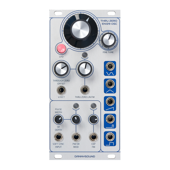
Dannysound – EN129 Thru Zero Oscillator
Build Guide v1.05
Contents
Section 1 - Main PCB
Resistors
Diodes
Inductors
IC Sockets
Capacitors
Transistors
Power Socket
Trim Pots
Electrolytic Capacitors
Board Connector
Section 2 – Power Test, Matched Transistors and IC placement
Section 3 – Pots PCB
Resistors
IC Sockets
Capacitors
Transistors
Panel Components
Calibration
Advertisement

Summary of Contents for Dannysound EN129 Thru Zero Oscillator
- Page 1 Dannysound – EN129 Thru Zero Oscillator Build Guide v1.05 Contents Section 1 - Main PCB Resistors Diodes Inductors IC Sockets Capacitors Transistors Power Socket Trim Pots Electrolytic Capacitors Board Connector Section 2 – Power Test, Matched Transistors and IC placement Section 3 –...
- Page 2 This build guide is for all kits and panel/pcb sets purchased BEFORE September 2020. The PCB bag label should be white, and on the front PCB it should be written ‘V1.0’ as circled below If you’re PCB reads v2.0 then please refer to build guide and BOM titled V2.0 https://www.thonk.co.uk/documents/dannysound/EN129_ThruZero/...
- Page 3 1 – Before starting on the main PCB, first locate the single 220R resistor and solder it into R214 on the front PCB. This designator is marked 1K but 220R is correct.
-
Page 4: Section 1 - Main Pcb
Section 1 - Main PCB Resistors 1 – 15 x 100k resistors... - Page 5 2 – 7 x 10k resistors...
- Page 6 3 – 6 x 1k resistors...
- Page 7 4 – 3 x 220k resistors...
- Page 8 5 – 3 x 2M2 resistors...
- Page 9 6 – 2 x 1k5 resistors...
- Page 10 7 – 2 x 1k8 resistors...
- Page 11 8 – 2 x 6k8 resistors...
- Page 12 9 – 2 x 470k resistors...
- Page 13 10 – 1 x 390r resistors...
- Page 14 11 – 1 x 2k2 resistors...
- Page 15 12 – 1 x 33k resistors...
- Page 16 13 – 1 x 150k resistors...
- Page 17 14 – 1 x 200k resistors...
- Page 18 15 – 1 x 56k resistors...
- Page 19 16 – 1 x 1M resistors...
- Page 20 17 – 1 x 8M2 resistors...
- Page 21 Diodes 18 – 3 x 1N4148 diodes – Note: orientation of this part is vital, be sure to match the line on the component with that on the PCB silkscreen...
- Page 22 Inductors 19 – 2 x bead inductors...
- Page 23 IC Sockets 20 – IC sockets – Make sure the notches in the sockets match the notches on the silkscreen.
- Page 24 Capacitors 21 – 1 x 47pF capacitor (located in diode bag)
- Page 25 22 – 12 x 100nF capacitors...
- Page 26 23 – 1 x 1nF polystyrene capacitor...
- Page 27 24 – 2 x 100pF capacitors...
- Page 28 Transistors 25 – 1 x MPF102 transistor – Orientation is vital - Ensure the flat face on the component matches the flat face on the PCB silkscreen. Be careful to individually identify all the transistors, there are many different types to separate, make sure what you have matches the label on the transistor bag.
-
Page 29: Power Socket
Power Socket 26 – 1 x power socket – make sure the slot is facing away from the edge of the PCB as indicated above. Orientation is vital! - Page 30 Trim Pots DO NOT PLACE HERE NOT REQUIRED FOR STANDARD THONK BUILD SINE TRIM SAW TRIM SINE SYM 27 – 3 x 100k blue trimpots (The ‘HFC’ trimpot is there as a precaution for high frequency correction, where the oscillator pitch tracks fine up to a certain point then starts to get flatter in the higher frequencies.
- Page 31 V/OCT 28 – 1 x 100r blue trimpot...
- Page 32 Electrolytic Capacitors 29 – 2 x 10uF capacitor - orientation is vital, the longer lead on the component should go to the circular pad marked with a plus ‘+‘ on the PCB. Note the component has a grey stripe on the cylindrical body on the minus side.
- Page 33 Board Connector 30 – Female connector...
-
Page 34: Section 2 - Power Test, Matched Transistors And Ic Placement
Section 2 – Power Test, Matched Transistors and IC placement Ground pin IC18 -12v pin 4 IC18 +12v pin 8 IC18 1 – test power... - Page 35 Take note of transistor orientation. Place transistors as close together as possible. 2 – 1 x matched pair of 2N3906s, both transistors have their flat edge facing towards C29. Orientation is vital. (The matched pair is located in the Panel/PCB bag)
- Page 36 3 – 1 x 2k TEMPCO resistor – solder the tempco so that it’s touching the matched pair below it...
- Page 37 4 – 5 x TL072 opamps – orientation is vital, for these opamps match the dot with the notch on the PCB silkscreen and IC Socket...
- Page 38 5 – 1 x TL074 opamp - match the notch on the chip with the notch on the PCB silkscreen and IC Socket - orientation is vital.
- Page 39 6 – 1 x CA3140 opamp - match the notch on the chip with the notch on the PCB silkscreen and IC Socket - orientation is vital...
- Page 40 7 – 2 x CA3080 opamps - match the notch on the chip with the notch on the PCB silkscreen and IC Socket - orientation is vital...
- Page 41 8 – 1 x CD4013 - match the notch on the chip with the notch on the PCB silkscreen and IC Socket - orientation is vital...
- Page 42 8 – 1 x CD4070 - match the notch on the chip with the notch on the PCB silkscreen and IC Socket - orientation is vital...
-
Page 43: Section 3 - Pots Pcb
Section 3 – Pots PCB Resistors 1 x 39K resistor... - Page 44 1 – 4 x 120k resistors...
- Page 45 R214 will already be filled with the 220R resistor that was soldered at the start of the build. 2 – 3 x 1k resistors...
- Page 46 3 – 2 x 100k resistors...
- Page 47 4 – 2 x 10k resistors...
- Page 48 5 – 1 x 2k2 resistor...
- Page 49 6 – 1 x 3k3 resistor...
- Page 50 7 – 1 x 22k resistor...
- Page 51 8 – 1 x 30k resistor...
- Page 52 9 – 1 x 150k resistor...
- Page 53 10 – 1 x 1M5 resistor...
- Page 54 11 – 1 x 5M6 resistor...
- Page 55 IC Sockets 12 – IC socket - Make sure the notch in the socket matches the notch on the silkscreen.
- Page 56 Capacitors 13 – 2 x 100nF capacitors...
- Page 57 14 – 5 x 10uF capacitors - orientation is vital, the longer lead on the component should go to the circular pad marked with a plus ‘+‘ on the PCB. Note the component has a grey stripe on the cylindrical body on the minus side.
- Page 58 15 – 1 x 1uF NP capacitor. This electro capacitor is non-polar so orientation does not matter.
- Page 59 Transistors 16 – 4 x 2N3904 transistors - Ensure the flat face on the component matches the flat face on the PCB silkscreen. Orientation is vital. Be careful to individually identify all the transistors, there are many different types to separate, make sure what you have matches the label on the transistor bag.
- Page 60 17 – 1 x 78L09 transistor - Ensure the flat face on the component matches the flat face on the PCB silkscreen. Orientation is vital.
- Page 61 18 – 1 x 79L09 transistor - Ensure the flat face on the component matches the flat face on the PCB silkscreen. Orientation is vital.
- Page 62 19 – 1 x SIL pin male header – now is also a good time to screw the four hex standoffs onto the front PCB...
- Page 63 20 – 1 x TL072 opamp - orientation is vital, match the dot with the notch on the PCB silkscreen and IC Socket...
-
Page 64: Panel Components
Panel Components These components should be inserted but NOT SOLDERED until the panel has been placed on top. This is to ensure that the PCB fits the panel properly. 21 – 3 x LEDs - orientation is vital, the shorter leg of the LED should go to the square pad and flat side of the PCB silkscreen diagram. - Page 65 The red dot on the black body of the pushbutton switch goes on this side 22 – 1 x Illuminated push button switch - orientation is vital.
- Page 66 23 – 3 x B100k blue body plastic shaft pots...
- Page 67 B100K 24 – 2 x B100K green body metal shaft pots...
- Page 68 Tune Fine Tune B10K B10K 25 - 2 x 10k linear alpha pots Note: If you have one longer shaft B10K pot this must go in the Tune position, if both shafts are the same length then they can both go in either position.
- Page 69 26 – 9 x jack sockets...
- Page 70 27 – Insert 1 x pot nut – this nut will sit below the panel...
- Page 71 28 – Insert LED light pipes and retainer clips...
- Page 72 29 – Fit the panel and insert second pot nut but do not fully tighten.
- Page 73 30 – Centre the knob with the panel graphics then remove the knob and tighten the nut. Now replace the knob again - screwing on with the supplied larger hex key. Note: be sure that the knob isn’t scraping against the panel.
- Page 74 31 – Solder one pin on each of the four outer jack sockets then add nuts to keep panel in place.
- Page 75 33 – Add knobs and solder one ground tab of each pot.
- Page 76 34 – Solder the LEDs in place making sure the LEDs are lined up and touching the light pipes. Check panel components are lined up properly and then solder the rest of the component pins on the PCB.
- Page 77 35 – Add PCB mounting hardware, connect the main board and insert the remaining screws.
- Page 78 Calibration This procedure requires an oscilloscope. V/OCT SINE TRIM SAW TRIM SINE SYM...
- Page 79 1 – Sine Symmetry Set the Frequency and Through Zero Offset controls to 50% and all other controls to 0. Connect the SINE output to the oscilloscope. Ensure the scope trace is centered. 1 – If the wave looks more square than triangle then adjust SINE TRIM to obtain more of a triangle wave shape.
- Page 80 2 – Sine Trim Adjust SINE TRIM again to produce a sine wave shape. If possible it’s a good idea to listen to the oscillator when making this adjustment as you might prefer a more rounded sine wave. 1 – Pure sine wave. 2 –...
- Page 81 3 – Saw Trim Connect the oscilloscope to the SAW output. Adjust SAW TRIM to obtain a saw wave.
- Page 82 V/OCT CALIBRATION The V/OCT calibration can be done using a guitar tuner or by listening if you have a good sense of pitch! 1 – Connect the SINE output to either an amplifier or a tuner. 2 – Connect voltage source / keyboard to V/OCT input. 3–...
Need help?
Do you have a question about the EN129 Thru Zero Oscillator and is the answer not in the manual?
Questions and answers