Table of Contents
Advertisement
Quick Links
Advertisement
Table of Contents

Subscribe to Our Youtube Channel
Summary of Contents for Terasic Apollo Carrier Board
- Page 1 Apollo Carrier Board www.terasic.com User Manual September 22, 2020...
-
Page 2: Table Of Contents
5.2 PC PCI Express Software SDK ......................29 5.3 PCI Express Software Stack ......................... 29 5.4 PCI Express Library API ........................34 5.5 PCIe Reference Design - DDR4......................39 Chapter 6 Transceiver Verification ................47 Apollo Carrier Board www.terasic.com User Manual September 22, 2020... - Page 3 6.1 Transceiver Test Code .......................... 47 6.2 QSFP28 Ports ............................47 6.3 40G Ethernet Example ......................... 48 Chapter 7 Additional Information................. 54 7.1 Getting Help ............................54 Apollo Carrier Board www.terasic.com User Manual September 22, 2020...
-
Page 4: Chapter 1 Overview
Apollo Carrier board and installation guide. 1.1 General Description Apollo Carrier board is a Carrier board design for Terasic Apollo S10 SoM board. Apollo Carrier board and Apollo S10 SoM board communication via FMC and FMC+ connectors. Apollo Carrier board provides 12V DC power for Apollo S10 via SAMTEC 2x6 connector. -
Page 5: Key Features
1.2 Key Features The following hardware is implemented on the Apollo Carrier board: Carrier board for Apollo S10 SoM Power input: 12V DC via PCIe 2x4 power connector Provides 12V DC to S10 via SAMTEC 2x6 power connector ... -
Page 6: Chapter 2 Board Components
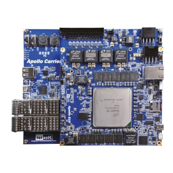
2.1 Board Overview Figure 2-1 is the top view of the Apollo Carrier Board. It depicts the layout of the board and indicates the location of the connectors and key components. Users can refer to this figure for relative location of the connectors and key components. -
Page 7: General User Input And Output
Figure 2-2 Position of 12V DC Input and Power Switch After Apollo S10 and Apollo Carrier Board are assembled, please: Always make Apollo S10 SoM power switch on. Do not use the 2x4 PCIe power connector on Apollo S10. - Page 8 GPIO ports is shown in Table 2-3 Table 2-4 shows all the pin assignments of the GPIO connector. The pin-out of JP1 is shown in Figure 2-4 Connection between 2x20 GPIO and Apollo S10 SoM Apollo Carrier Board www.terasic.com User Manual September 22, 2020...
- Page 9 Figure 2-5 Location of the JP2 Table 2-2 Header setting for I/O standard of the JP2 JP2 Setting FMC I/O Standard 3.3V(Default Setting) 2.5V Apollo Carrier Board www.terasic.com User Manual September 22, 2020...
- Page 10 1.8V Figure 2-6 Pin 1 of the GPIO header Figure 2-7 Pin-out of 2x20 GPIO Header JP1 Apollo Carrier Board www.terasic.com User Manual September 22, 2020...
- Page 11 PIN_F21 FMC_GPIO_D[24] GPIO Connection[24] 3.3(Default)/2.5/1.8V PIN_B18 FMC_GPIO_D[25] GPIO Connection[25] 3.3(Default)/2.5/1.8V PIN_F20 FMC_GPIO_D[26] GPIO Connection[26] 3.3(Default)/2.5/1.8V PIN_B19 FMC_GPIO_D[27] GPIO Connection[27] 3.3(Default)/2.5/1.8V PIN_C17 FMC_GPIO_D[28] GPIO Connection[28] 3.3(Default)/2.5/1.8V PIN_A22 FMC_GPIO_D[29] GPIO Connection[29] 3.3(Default)/2.5/1.8V PIN_P23 Apollo Carrier Board www.terasic.com User Manual September 22, 2020...
-
Page 12: Clock Generator
Si5340A_I2C_SCL 1.8V PIN_AU34 clock generator I2C data bus of the 1.8V Si5340A_I2C_SDA PIN_AU33 clock generator Enable output of the 1.8V SI5340A_OE_n PIN_BG38 clock generator SI5340A_RST_n Reset of the clock 1.8V PIN_BG37 Apollo Carrier Board www.terasic.com User Manual September 22, 2020... -
Page 13: Qsfp28 Ports
DIFFERENTIAL I/O QSFP28A_RX_p[1] Receiver data of channel 1 HSSI PIN_AH4 DIFFERENTIAL I/O QSFP28A_RX_p[2] Receiver data of channel 2 HSSI PIN_AF4 DIFFERENTIAL I/O QSFP28A_RX_p[3] Receiver data of channel 3 HSSI PIN_AG4 DIFFERENTIAL I/O Apollo Carrier Board www.terasic.com User Manual September 22, 2020... - Page 14 DIFFERENTIAL I/O QSFP28B_TX_p[1] Transmitter data of channel 1 HSSI PIN_G47 DIFFERENTIAL I/O QSFP28B_TX_p[2] Transmitter data of channel 2 HSSI PIN_E47 DIFFERENTIAL I/O QSFP28B_TX_p[3] Transmitter data of channel 3 HSSI PIN_C47 DIFFERENTIAL I/O Apollo Carrier Board www.terasic.com User Manual September 22, 2020...
-
Page 15: Pci Express
HSSI DIFFERENTIAL I/O PIN_BE43 PCIE_TX_p[0] Transmit bus HSSI DIFFERENTIAL I/O PIN_BJ46 PCIE_TX_p[1] Transmit bus HSSI DIFFERENTIAL I/O PIN_BF45 PCIE_TX_p[2] Transmit bus HSSI DIFFERENTIAL I/O PIN_BG47 PCIE_TX_p[3] Transmit bus HSSI DIFFERENTIAL I/O PIN_BE47 Apollo Carrier Board www.terasic.com User Manual September 22, 2020... -
Page 16: Usb Downstream Port
2.7 USB Downstream Port The Thunderbolt 3 controller on the Apollo carrier board not only allows the FPGA and Host PC to establish PCIe interface connections through a Thunderbolt 3 cable, but also provides another expansion port for a USB downstream port (See Figure 2-11). - Page 17 Figure 2-12 Connection setup for USB downstream port (Carrier board) to USB Blaster II Port (Module board) Figure 2-13 JTAG connection via USB downstream port Apollo Carrier Board www.terasic.com User Manual September 22, 2020...
-
Page 18: Chapter 3 Board Assembly
Figure 3-1, is used for board stacking. Four JSOM standoff are required to assemble Apollo S10 SoM and Apollo Carrier Board. Each JSOM standoff is consistent with four components. The Apollo S10 kit includes four JSOM standoff as shown in Table 3-1. -
Page 19: Assembly
1.5mm Hex Key 5.0mm Hex Socket 3.2 Assembly Below are the procedures to assemble the Apollo S10 SoM and Apollo Carrier Board or user can “How to assemble Apollo S10 with carrier refer to the video board” to assemble the board. - Page 20 Figure 3-2 Assemble M2.5 Screws and JSOM-B on Apollo S10 Figure 3-3 Assemble JSOM-T to JSOM-B Figure 3-4 Place Apollo Carrier Board over four JSOM-T Apollo Carrier Board www.terasic.com User Manual September 22, 2020...
-
Page 21: Disassembly
Figure 3-5 Push Apollo Carrier Board onto JSOM-T Figure 3-6 Assemble Hex Nut to JSOM-T 3.3 Disassembly Here are the procedures to disassemble with Apollo S10 SoM and Apollo Carrier Board or users can refer to the video “How to disassemble Apollo S10 with carrier board”... - Page 22 Figure 3-7 Disassemble Hex Nut Figure 3-8 Disassemble JSOM-T to JSOM-B Apollo Carrier Board www.terasic.com User Manual September 22, 2020...
- Page 23 Figure 3-9 Unscrew JSOM-B Apollo Carrier Board www.terasic.com User Manual September 22, 2020...
-
Page 24: Setup Thunderbolt 3
Chapter 4 Setup Thunderbolt 3 hunderbolt 3 is unique communication path between the Host PC and Apollo Carrier board. As shown in Figure 4-1, while the Apollo S10 SoM is connected to the carrier board to form the Apollo Developer Kit. With a Thunderbolt 3 cable, Host PC can communicate with the FPGA on the developer kit via PCIe protocol (PCIe design is required in the FPGA). -
Page 25: Thunderbolt 3 Test On Windows Os
An Apollo Developer Kit (Apollo S10 SoM + Apollo Carrier board) A Thunderbolt 3 Cable as shown in Figure 4-2 Figure 4-2 Thunderbolt 3 Cable 4.2 Thunderbolt 3 Test on Windows OS Below shows the procedure when the Apollo Developer Kit is first time to plug into the Thunderbolt 3 port of the Host PC. - Page 26 3_connection_win10 4-5. Select “Always Connected” A Thunderbolt Dialog window will appear as shown in Figure and click OK button. Apollo Carrier Board www.terasic.com User Manual September 22, 2020...
-
Page 27: Detect Pcie Device In The Fpga
User first needs to program the PCIe design to the FPGA, then re-establish the Thunderbolt 3 connection to the Host that allow the Host to detect the PCIe device in the FPGA. Below we introduce the use of a Terasic PCIe demo to demonstrate the detection of a PCIe device on the Host. - Page 28 PCI device does not appear in the Device Manager, please re-plug the Thunderbolt cable again then check again. Next, to install the PCIe driver for FPGA design, please refer to the section 5.3 for detailed. Figure 4-6 PCI Device in the Device Manager Apollo Carrier Board www.terasic.com User Manual September 22, 2020...
-
Page 29: Pci Express Reference Design For Windows
FPGA System and PC System. The FPGA System is developed based on Stratix 10 Hard IP for PCI Express with Avalon-MM DMA. The application software on the PC side is developed by Terasic based on Altera’s PCIe kernel mode driver. Figure 5-1 Infrastructure of PCI Express System Apollo Carrier Board www.terasic.com... -
Page 30: Pc Pci Express Software Sdk
The PCIe library module TERASIC_PCIE_AVMM.dll provides DMA and direct I/O access allowing user application program to communicate with FPGA. Users can develop their applications based on this DLL. The altera_pcie_win_driver.sys kernel driver is provided by Intel. Apollo Carrier Board www.terasic.com User Manual... - Page 31 Device Manager to launch the Device Manager dialog. There will be a PCI Device item in the dialog, as shown in Figure 5-3. Move the mouse cursor to the PCI Apollo Carrier Board www.terasic.com User Manual September 22, 2020...
- Page 32 6. In the How do you want to search for the driver software dialog, click Browse my computer for driver software item, as shown in Figure 5-4. Figure 5-4 Dialog of Browse my computer for the driver software Apollo Carrier Board www.terasic.com User Manual September 22, 2020...
- Page 33 Figure 5-6 Click Install in the dialog of Windows Security 9. When the driver is installed successfully, the successfully dialog will appear, as shown in Figure 5-7. Click the Close button Apollo Carrier Board www.terasic.com User Manual September 22, 2020...
- Page 34 10. Once the driver is successfully installed, users can see the Altera PCI API Driver under the device manager window, as shown in Figure 5-8 Figure 5-8 Altera PCI API Driver in Device Manager Apollo Carrier Board www.terasic.com User Manual September 22, 2020...
-
Page 35: Pci Express Library Api
Specify the desired device ID. A zero value means to ignore the device ID. wCardIndex: Specify the matched card index, a zero based index, based on the matched vendor ID and Apollo Carrier Board www.terasic.com User Manual September 22, 2020... - Page 36 Parameters: hPCIE: A PCIe handle return by PCIE_Open function. PcieBar: Specify the target BAR. PcieAddress: Specify the target address in FPGA. pdwData: A buffer to retrieve the 32-bit data. Return Value: Apollo Carrier Board www.terasic.com User Manual September 22, 2020...
- Page 37 Read an 8-bit data from the FPGA board. Prototype: bool PCIE_Read8( PCIE_HANDLE hPCIE, PCIE_BAR PcieBar, PCIE_ADDRESS PcieAddress, uint8_t *pByte); Parameters: hPCIE: A PCIe handle return by PCIE_Open function. PcieBar: Specify the target BAR. PcieAddress: Apollo Carrier Board www.terasic.com User Manual September 22, 2020...
- Page 38 PCIE_DmaRead Function: Read data from the memory-mapped memory of FPGA board in DMA. Maximal read size is (4GB-1) bytes. Prototype: bool PCIE_DmaRead( PCIE_HANDLE hPCIE, PCIE_LOCAL_ADDRESS LocalAddress, void *pBuffer, uint32_t dwBufSize Parameters: Apollo Carrier Board www.terasic.com User Manual September 22, 2020...
- Page 39 Return true if write data is successful; otherwise false is returned. PCIE_ConfigRead32 Function: Read PCIe Configuration Table. Read a 32-bit data by given a byte offset. Prototype: bool PCIE_ConfigRead32 ( Apollo Carrier Board www.terasic.com User Manual September 22, 2020...
-
Page 40: Pcie Reference Design - Ddr4
5. Pull the Thunderbolt 3 cable off form the Host, then pull the cable in again for redetect the PCIe device 6. Make sure that Windows has detected the FPGA Board by checking the Windows Device Manager as shown in Figure 5-9 Apollo Carrier Board www.terasic.com User Manual September 22, 2020... - Page 41 9. Type 2 followed by the ENTER key to select the Link Info item. The PCIe link information will be shown as in Figure 5-11. Gen3 link speed and x3 link width are expected. Apollo Carrier Board www.terasic.com User Manual September 22, 2020...
- Page 42 11. Type 4 followed by the ENTER key to select the DMA DDR4A Bank Memory Test item. The DMA write and read test result will be reported as shown in Figure 5-13 Apollo Carrier Board www.terasic.com User Manual September 22, 2020...
- Page 43 12. Type 5 followed by the ENTER key to select the DMA DDR4B bank Memory Test item. The DMA write and read test result will be reported as shown in Figure 5-14 Apollo Carrier Board www.terasic.com User Manual September 22, 2020...
- Page 44 13. Type 99 followed by the ENTER key to exit this test program. Development Tools Quartus Prime 19.1 Pro Edition Visual C++ 2012 Demonstration Source Code Location Quartus Project: Demonstrations\PCIE_DDR4 Visual C++ Project: Demonstrations\PCIe_SW_KIT\Windows\PCIe_DDR4 Apollo Carrier Board www.terasic.com User Manual September 22, 2020...
- Page 45 Implement dynamically load for TERAISC_PCIE_AVMM.DLL PCIE.h TERASIC_PCIE_AVMM.h SDK library file, defines constant and data structure The main program PCIE_DDR4.cpp includes the header file "PCIE.h" and defines the controller address according to the FPGA design. Apollo Carrier Board www.terasic.com User Manual September 22, 2020...
- Page 46 PCIE_Read32 API, as shown below: he memory-mapped memory read and write test is implemented by PCIE_DmaWrite and PCIE_DmaRead API, as shown below: Apollo Carrier Board www.terasic.com User Manual September 22, 2020...
- Page 47 The PCIe link information is implemented by PCIE_ConfigRead32 API, as shown below: Apollo Carrier Board www.terasic.com User Manual September 22, 2020...
-
Page 48: Chapter 6 Transceiver Verification
To enable an external loopback of the transceiver channels, QSFP28 loopback fixtures, as shown in Figure 6-1, are required. The fixture is available at: https://multilaneinc.com/product/ml4002-28/ Figure 6-1 QSFP28 Loopback fixtures Figure 6-2 shows the FPGA board with four QSFP28 loopback fixtures installed. Apollo Carrier Board www.terasic.com User Manual September 22, 2020... -
Page 49: Ethernet Example
This example executes the external loopback test through one of the QSFP28 ports on the FPGA main board. A QSFP28 loopback fixture is required to perform this demonstration. Figure 6-3 shows the block diagram of this demonstration. Apollo Carrier Board www.terasic.com User Manual September 22, 2020... - Page 50 The run_test is used to enable transceiver serial loopback for internal loopback. Make sure your Host PC has installed the Quartus 19.4 Pro edition. Insert a QSFP28 loopback fixture into the QSFP28-A port on the Apollo carrier board, as shown in Figure 6-2.
- Page 51 “test.bat” to program the FPGA and run the Tcl file (See Figure 6-4). The Tcl file will open the Quartus tool “System Console” automatically(See Figure 6-5). Figure 6-4 Execute demo batch file Apollo Carrier Board www.terasic.com User Manual September 22, 2020...
- Page 52 Figure 6-5 Launch the System Console for Ethernet 40G Demo If you have a QSFP28 loopback fixture installed, type “loop_off” to turns off internal serial loopback. Otherwise, type “loop_on” to turn on internal serial loopback(See Figure 6-6). Apollo Carrier Board www.terasic.com User Manual September 22, 2020...
- Page 53 Figure 6-6 Enter command for test Type “start_pkt_gen” to starts the packet generator. Type “chkmac_stats” to display the values in the MAC statics counters, as shown in Figure 6-7. Apollo Carrier Board www.terasic.com User Manual September 22, 2020...
- Page 54 Figure 6-7 Ethernet 40G loopback test report for RX and TX Apollo Carrier Board www.terasic.com User Manual September 22, 2020...
-
Page 55: Chapter 7 Additional Information
First publication 2020.04 V1.1 Add chapter 5 &6 2020.05 V1.2 Add assemble and disassemble board video in chapter 3 2020.06 V1.3 Fix some description error 2020.09 V1.4 Fix some description error Apollo Carrier Board www.terasic.com User Manual September 22, 2020...
Need help?
Do you have a question about the Apollo Carrier Board and is the answer not in the manual?
Questions and answers